

Welcome to the 53rd investment case, 43rd Resilience & Quality, 30th Reshoring & Sovereignty, 26th AI & Technology idea on Crack the Market (and the most comprehensive TSMC investment case you will find online)! Join me as I dissect the most important company in the world, a famously conservative compounder that has transformed itself into a Foundry 2.0 system integrator and now sits at the crossroads of our digitalizing world, advanced packaging, and geopolitical strategy, and is riding a generational wave of artificial intelligence infrastructure and global supply chain reshoring.
Twice a week, I will release deep dives into stocks and sectors that fit into the 6 themes that I see winning in the coming years and decades: AI & Technology, Electrification & Energy, Reshoring & Sovereignty, Healthcare & Longevity, China & Asia, Resilience & Quality.
Take advantage of this once in a generation opportunity to build long term wealth by investing in great stocks that will deliver returns for your portfolio for years to come.
After reading this article, you will understand why TSMC is arguably the most important company in the world, acting as the architectural toll booth of the AI era. You will discover how it has evolved from a cyclical business into a structural growth compounder, why its dominance in advanced packaging and leading-edge nodes creates an unbreachable moat, and why it remains one of the best businesses to own for the next decade as it captures the value of the AI revolution.
In this article I go through:
TSMC’s business and how it dominates the global foundry market with a near-monopoly on leading-edge manufacturing and building AI accelerators.
A deep dive into what chips are, how they are made and how the semiconductor sector is structured between fabless and foundries.
How the company has transitioned to Foundry 2.0, integrating wafer fabrication with advanced packaging to become the indispensable bottleneck of the AI supply chain.
How the company aims to deliver 25% revenue CAGR through 2029, driven by unprecedented demand from hyperscalers.
How its unique pricing power and manufacturing excellence allow it to maintain software-like margins despite massive capital intensity.
Why its valuation is at an inflection point, rerating from a cyclical multiple to a structural growth multiple supported by a conservative yet high-performing management team
TSMC Investment Case
Table of content
Business Description
Taiwan Semiconductor Manufacturing (TSMC) was established in 1987 as a provider of semiconductor foundry services. TSMC manufactures semiconductors using its own manufacturing process for customers based on proprietary integrated circuit (IC) designs that customers provide. By choosing not to design, manufacture or market any semiconductor products under its own name, TSMC ensures it never competes with its customers. TSMC’s foundry business model has led to the rise of the global fabless industry. TSMC now has a market cap of TWD 45.9tn or $1.46tn (6th biggest company in the world).
TSMC today offers design, advance packing services, mask making, testing, foundry and cyber shuttle services. The company also offers several logic and specialty technologies. TSMC represented 34 % of the Foundry 2.0 industry in 2024, as compared to 28 % in 2023. This refers to TSMC’s share of the Foundry 2.0 industry, defined by TSMC as all logic wafer manufacturing, packaging, testing, mask-making, and other output value.
TSMC is the largest foundry globally, with a dominant market share of 70-72% as of Q4 2025. TSMC’s products underpin the entire digital economy and the world around us. They find use in a wide range of applications including high-performance computing, smartphones, digital consumer electronics, internet of things (loT), and automobiles. Headquartered in Hsinchu, Taiwan, the company also has operations in North America (which are quickly expanding), Europe and Asia Pacific including Japan, India, China, and South Korea.
Geographical breakdown (2024):
North America: 70% of sales
China: 11% of sales
Asia Pacific: 10% of sales
Japan: 5% of sales
EMEA: 4% of sales.
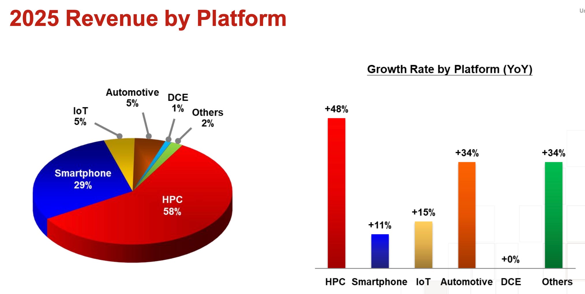
Platform breakdown (2025):
High Performance Computing (HPC): 58% of sales
Smartphone: 29% of sales
Internet of Things (IoT): 5% of sales
Automotive: 5% of sales
Digital Consumer Electronics: 1% of sales
Other: 2% of sales
TSMC’s customers are mainly fabless semiconductor companies (which only design the chip which TSMC then manufactures for them)/electronics companies (which have begun designing their own silicon in recent years). Apple remained TSMC’s largest customer, accounting for 22% of net revenue in 2024. Nvidia followed as the second-largest client, with 12% of TSMC’s net revenue. Other major customers include AMD, Qualcomm, MediaTek, Broadcom, and Intel.
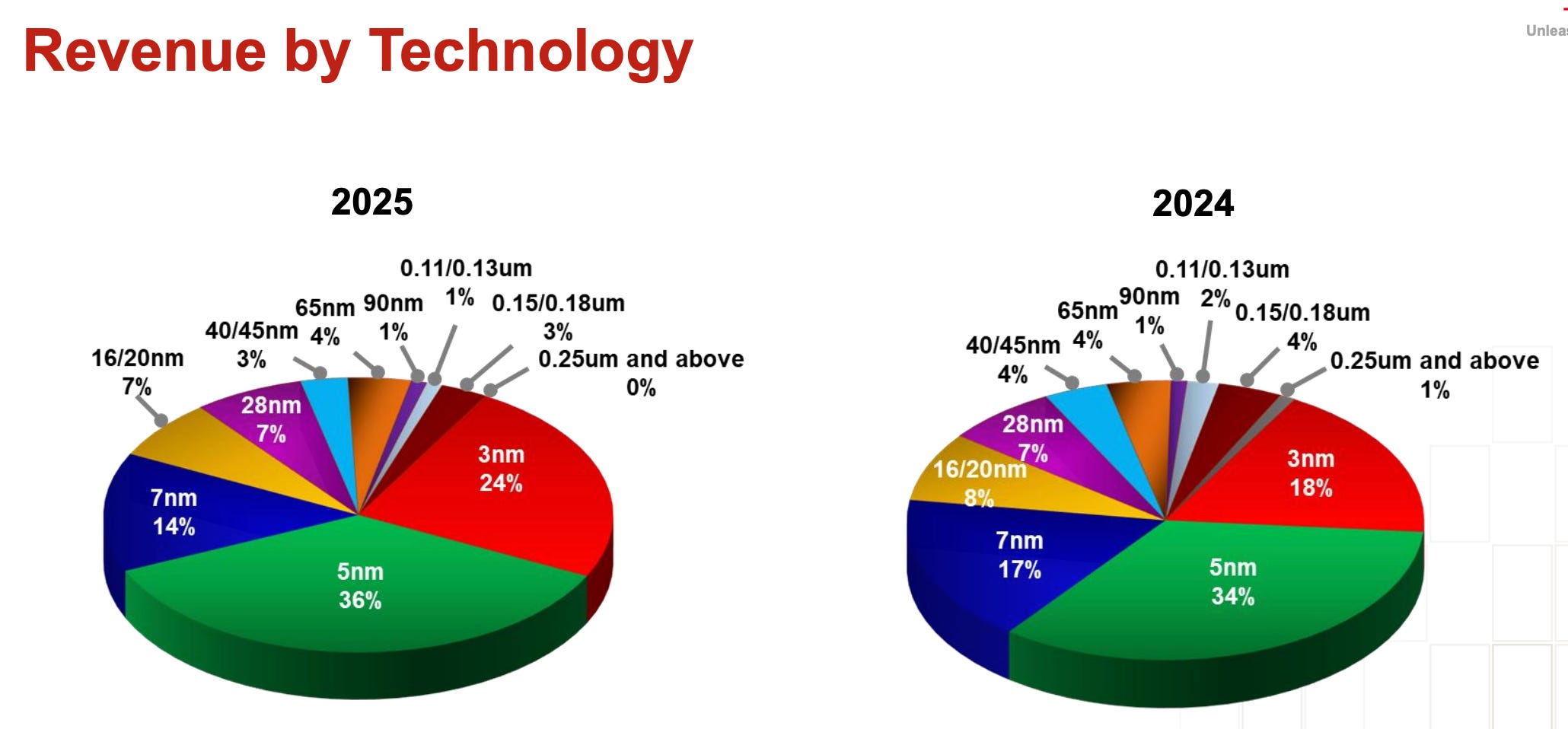
Technology breakdown:
3nm: 24% of sales
5nm: 36% of sales
7nm: 14% of sales
16nm: 7% of sales
28nm: 7% of sales
40/45nm: 3% of sales
65nm: 4% of sales
Rest: 5% of sales
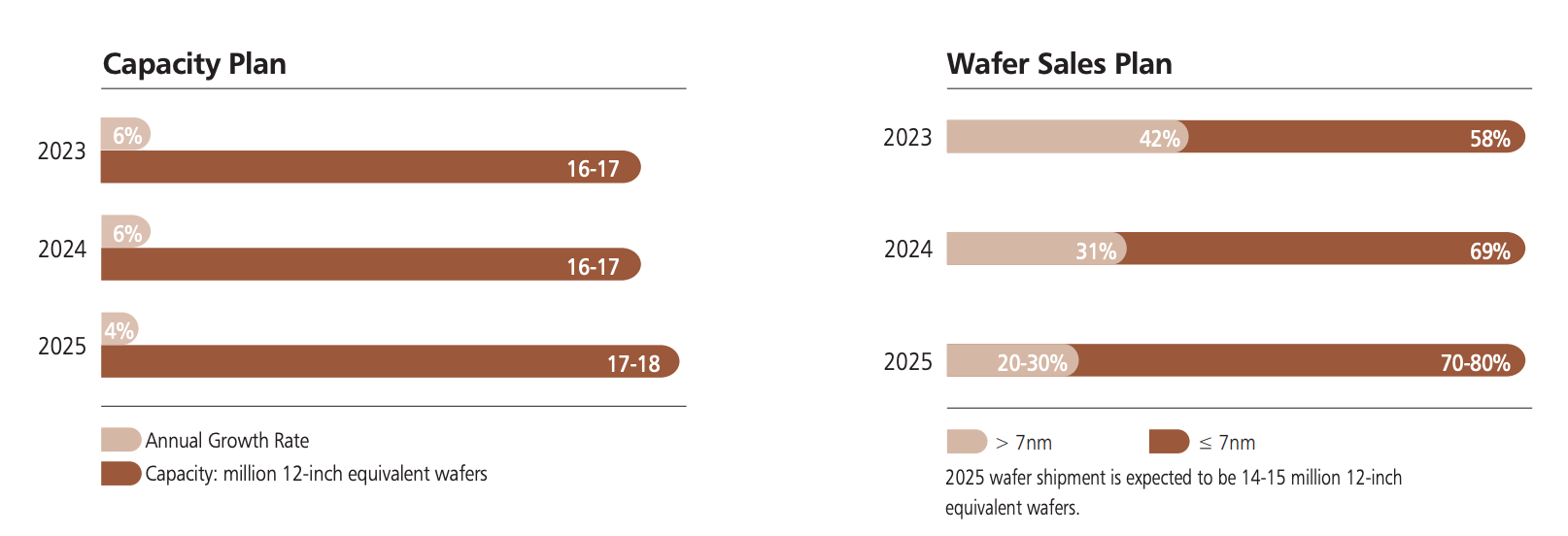
TSMC’s yearly capacity breakdown by node (around 18m wafers per year):
2nm: 500k
3nm: 1,500k
5nm: 1,800k
7nm: 1,800k
10nm: 300k
16nm: 1,500k
20nm: 200k
28nm: 2,000k
40nm: 1,500k
65nm: 1,500k
90nm: 1,150k
8-inch fabs: 4,000k
US fabs: 200k
Japan fabs: 350k
Taiwan - The Home Base (total around 1,400kWpm, overview of major TSMC fabs, creating the most important semiconductor cluster in the world in Taiwan):
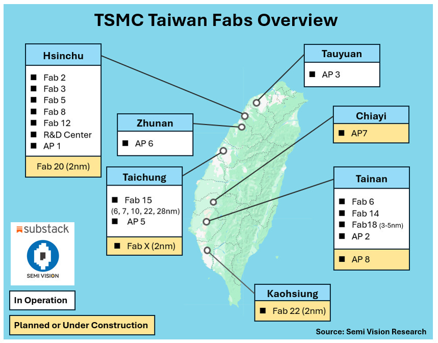
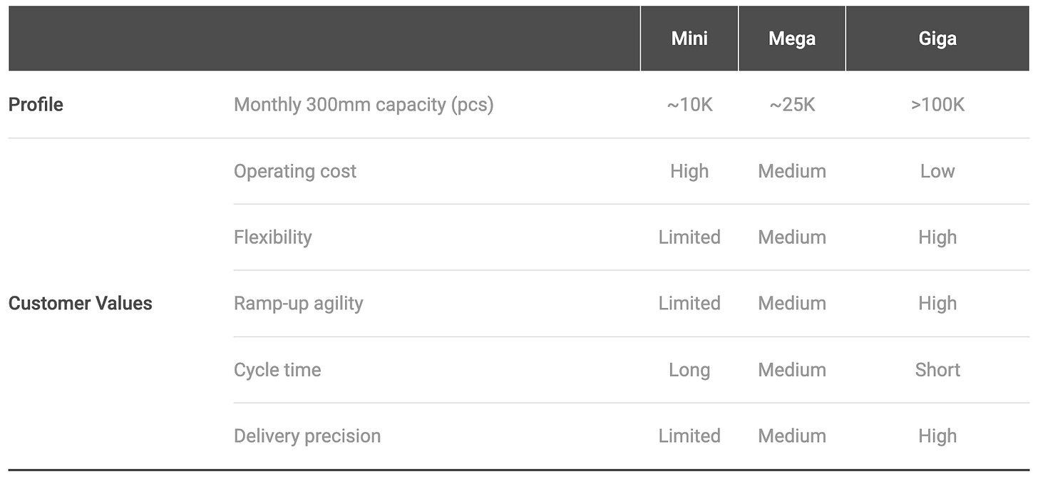
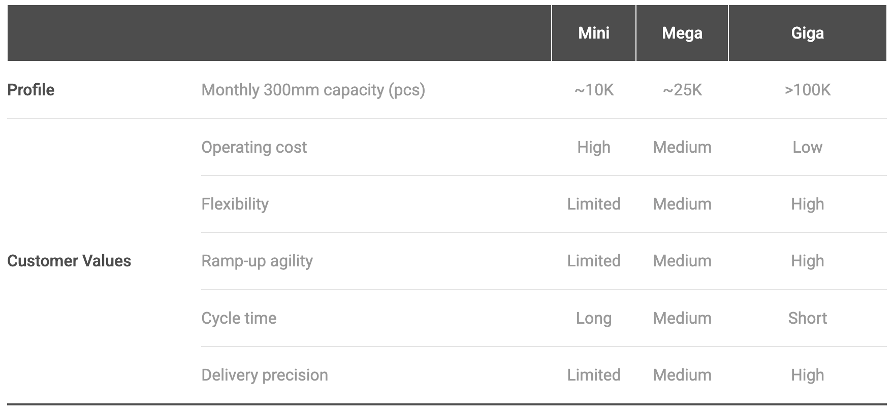
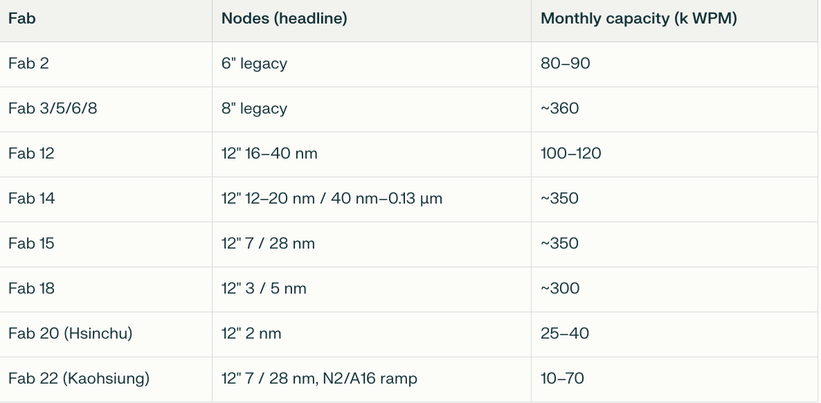
TSMC mostly runs Gigafabs, facilities with >100kWpm (cities making the world’s most important products) with a total output of 12.7 million wafers per year: Maintaining reliable production capacity is a key manufacturing strategy at TSMC: TSMC currently operates four 12-inch GIGAFAB facilities: Fab 12, 14, 15 and 18. The combined capacity of the four facilities exceeded 12.74 million 12-inch wafers in 2024. Production within these facilities support 0.13μm, 90nm, 65nm, 40nm, 28nm, 16nm, 7nm, 5nm and 3nm process technologies and their sub-nodes. The GIGAFAB facilities are coordinated by a centralized management system known as super manufacturing platform (SMP) to provide customers with consistent quality and reliability, greater flexibility to cope with demand fluctuations, and faster yield learning and time-to-volume production, as well as better-function and lower-cost product requalification.
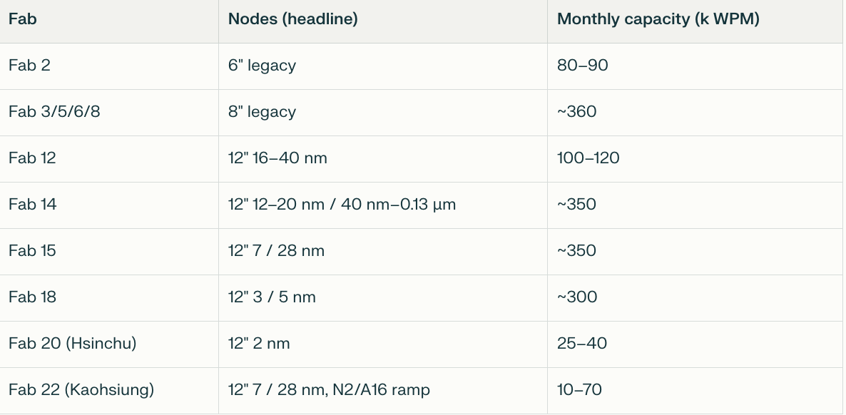
TSMC’s front end capacity around 18m wafers per year(by most recent processes):
Fab 23 (A14): TBD
Fab 22 (N2/A16): 10kWpm going towards 70kWpm
Fab 20 (N2): 25kWpm going towards 40kWpm
Fab 18 (N5/N3): 285kWpm going towards 290kWpm (Gigafab)
Fab 15 (7-28nm): 350kWpm (Gigafab)
Fab 14 (12/40nm): 350kWpm (Gigafab)
Fab 12 (16/40nm): 100-120kWpm (Gigafab)
Fab 3/5/6/8 (8 inch): 360kWpm
Fab 2 (6 inch): 80-90kWpm
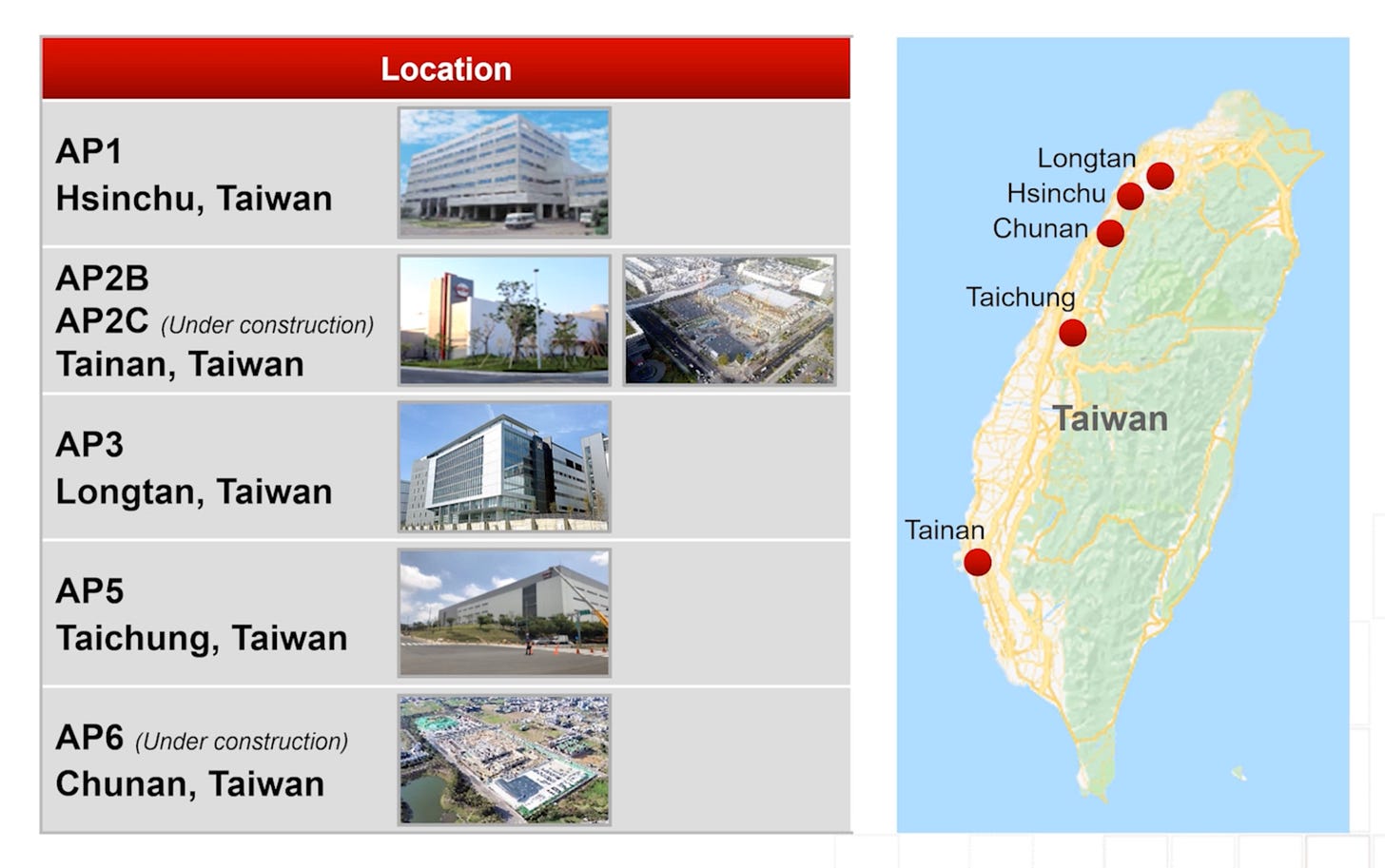
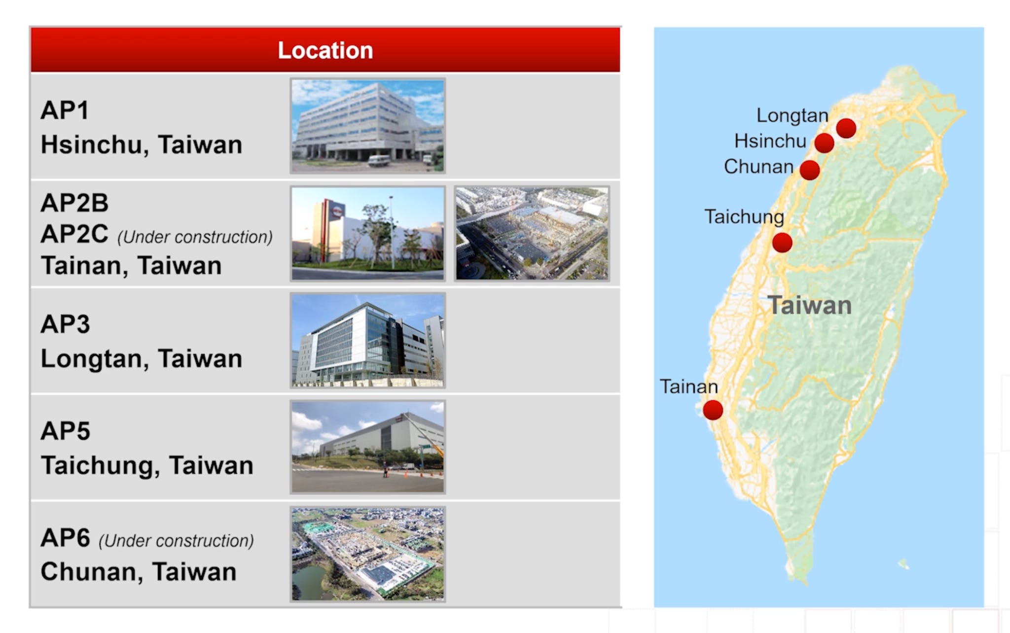
Advanced packaging plants (becoming more and more important): In 2024, TSMC established 2nm advanced manufacturing facilities in Hsinchu and Kaohsiung, and expanded advanced packaging capabilities in Chiayi and Tainan. These efforts help clients accelerate innovation to meet the rapidly changing market challenges and satisfy greater demand brought by the growth of AI.
Overseas expansion meets reshoring ambitions - a structural growth driver mitigating geopolitical risks:
To better serve the needs of global customers, TSMC has made significant progress at several overseas production sites, such as those in Arizona, US, and Kumamoto, Japan, enhancing the maturity and stability of its global operations.
US fabs in Arizona may generate lower ROIC than Taiwan-based fabs, but their strategic value is immense: They serve as geopolitical insurance, tariff mitigation, and customer lock-in mechanisms. Customers are willing to pay a premium for supply-chain security. Meanwhile, expansion in Japan is proceeding rapidly, with strong government support. Taiwan’s domestic expansion is supported by assurances on power infrastructure, reflecting TSMC’s role as the island’s silicon shield.
Time to reshore advanced semi production: Geopolitical risks have become the primary concern that has been pushing TSMC’s overseas expansion to reduce reliance on production in Taiwan and safeguard against potential disruptions of the current supply chain. In addition, this overseas expansion is driven by the global reshoring trend, especially in the US, with the US government (and some companies) looking to localize the production of their chips domestically. The US is moving towards producing 20-25% of all advanced chips on its soil after years of decline and near irrelevance in this space, a particularly important capability given the rising tensions globally, and TSMC is at the center of this effort. This is also linked to the AI revolution and race between the US and China. The US is slowly building an entire domestic AI supply chain (with Blackwells now partly produced in Arizona).
TSMC is simultaneously building new facilities in the US, Europe and Japan, with the focus being overwhelmingly on the US. The advanced-node wafer production from the overseas fabs could account for 20% of TSMC’s global advanced-node wafer production at the end of this decade.
TSMC’s global expansion plan so far:
Japan: Kumamoto Fab 23 mature node + leading edge (55kWpm 2024 + 45kWpm 2027)
Europe: Dresden Fab mature node (40kWpm 2027)
US: Arizona Fab 21 leading edge (20kWpm 2025 + 30kWpm 2027 + 25kWpm 2030 + around 75kWpm beyond)
Becoming America’s fab - Arizona hub (Fab 21 total 75kWpm):
Towards a US AI supply chain: TSMC’s US expansion is part of a broader push to build a global hub in the US in response to geopolitical and supply chain risks, ultimately creating a US AI supply chain, though Taiwan remains central for cutting-edge lead nodes.
An ever growing US manufacturing hub: TSMC’s Arizona presence has grown from a single fab into a cluster of multiple fabs under an original $65 billion investment plan for three fabs ($14bn, $26bn and $28bn), supported by the CHIPS Act and corporate funding. TSMC has sinced expanded its total US investment to roughly $165 billion (in Mar 25), including three additional fabs (likely 80-90% of the amount are for these fabs: maybe 75kWpm of the A16 process or below), packaging facilities, and an R&D center. Even more recently, as part of a trade deal between the US and Taiwan, and linked to the very strong demand for AI chips and tight foundry capacity, TSMC has bought more land around its Arizona cluster with potential total US investments heading towards $300bn.
Fab production timelines - US production ramping up nicely:
First fab (N4/4nm) 20kWpm already started volume production in the first half of 2025.
A second fab (3/2nm) 30kWpm is already planned to start commercial production around H1 2027 (being sped up), producing 3nm and 2nm semiconductors, including the advanced 2 nm for AI/logic products.
Third fab 25kWpm will focus on 2 nm or more advanced nodes with production by the end of the decade.
Symbolic milestone: TSMC has already marked a milestone in Arizona by producing its first US made Blackwell AI chips in 2025, signaling progress on local advanced manufacturing, a key reshoring indicator.
It is more expensive to produce in the US than in Taiwan - impacting TSMC’s long term profitability: TSMC’s fabs in the US (cutting edge) vs Taiwan, for a similar capacity, are 80% more expensive (capex) than that for a comparable fab in Taiwan. Although the prices of utilities (mainly electricity) are much higher in Taiwan than in Arizona (>50%), TSMC’s Arizona fab pays engineers 3-5x higher salaries than in Taiwan. Despite some subsidies, TSMC’s US wafers will be 40% more expensive than those produced in Taiwan. Therefore, to maintain the same gross margin as for wafers shipped from Taiwan, TSMC may need to hike prices of its US-manufactured wafers by as much as 35-40%, which is doing thanks to the shortage of capacity and massive demand for AI and advanced chips. Still, some investors expected a gross margin erosion medium-long term and a ROIC impacted by the US fabs as they start making up a bigger part of TSMC’s global mix. But the company’s incredible pricing power should keep gross margins around 60% long term and ROE at 20%, truly impressive (something I discuss more in the Financials part).
Update Q4 25:
First fab entered high-volume production in Q4 24
Construction of 2nd fab is complete, and tool moving & installation planned in 2026, expect high-volume manufacturing in H2 2027
Construction of 3rd fab already started and in process of applying for permits for 4th fab construction
They recently bought a second large piece of land next to the existing cluster to support the current expansion plan.
Japan and Europe reshoring also in progress, but with much more modest goals:
Fabs in Japan (Fab 23 total 100kWpm):
In Nov 2021, TSMC, Sony Semiconductor Solutions (SSSC) established a JV, Japan Advanced Semiconductor Manufacturing (JASM), in Kumamoto, Japan, which is majority-owned by TSMC.
The first fab began volume production with a capacity of 55kWpm and mostly offering 22/28 nm processes for specialty technologies.
In Feb 2024, TSMC, SSSC, Toyota and Denso announced further investments in the JV JASM and plans for a second fab at Kumamoto (Feb 24) have been greenlit and construction is ongoing (started in Q1 25) for $12bn. It is scheduled to begin operations by the end of 2027 with capacity targeted at 40 nm through 6/7 nm nodes, serving automotive, industrial, and specialty applications. The second fab is estimated to have a capacity of 45kWpm, focusing on 12nm/16nm and 6nm/7nm process technologies for automotive, industrial, consumer and HPC-related applications.
from 40, 22/28, 12/16 and 6/7 nanometer process technologies for automotive, industrial, consumer and HPC-related applications.
Total Kumamoto capacity: 100kWpm. Total investment in JASM’s Kumamoto site (both fabs) is estimated to exceed $20 billion, with strong support from the Japanese government of originally $3bn but recently increased to $7bn.
Potential for cutting edge conversion: For now, the Japanese fabs are centered on mature and specialty nodes (from 40 nm up to 6/7 nm) rather than cutting-edge leading logic (2–3 nm). There are reports that TSMC and JASM are evaluating potential process upgrades (moving toward 4 nm capabilities at future phases) to meet evolving demand, though these discussions are ongoing and not yet finalized.
Fabs in Europe (Dresden Fab total 40kWpm):
TSMC’s Europe fab is located at Dresden, Germany. The fab was built by European Semiconductor Manufacturing Company (ESMC), a JV between TSMC, Bosch, infineon and NXP that was established in 2023. The total investment in the ESMC lab is EUR10bn, with roughly half of the project’s cost covered by government subsidies.
The fab is expected to start production by the end of 2027 with an initial capacity of 40kWpm (300mm wafer). The fab will primarily focus on chips for Germany’s automotive industry, using TSMC’s 12nm, 16nm, 22nm, and 28nm class process technologies (key nodes for automotive and industrial chips). This facility will be Europe’s first FinFET-capable pure-play foundry
and is being supported by the European Commission and German government, including a reported EUR5 billion state aid package.
TSMC’s European moves align with EU goals to strengthen semiconductor supply chains and reduce dependency on East Asia. The Dresden facility is a cornerstone of that effort and is significant because it brings advanced wafer manufacturing technology (FinFET nodes) into the EU for the first time at scale.
TSMC is considering building more fabs in Europe.
