


ASML: The most innovative company in the world will 2.5x its EPS by 2030
The benevolent monopoly

Welcome to the 1st investment case, and 1st resilience, reshoring/sovereignty, China, AI & data center idea on Crack the Market (and the most comprehensive ASML investment case you will find online)! Join me as I dissect the most important company in the world, at the heart of the semiconductor value chain, which enables the whole digital world around us from smartphones and AI to industry and automotive.
As the first investment deep dive that I am publishing, I am making this available to everyone to give you a flavour of what you can expect as a subscriber for dozens of other companies and trends in the next few weeks and months.
Going forward, everyone will have access to a teaser for every future company article I publish (every week) and megatrend articles with the associated stocks (every month). For subscribers you will a deep dive into a company every week, a megatrend analysis with a deeper breakdown and a granular analysis of the stocks exposed to the theme, and access to a me, a portfolio management professional, for your questions.
Twice a week, I will release deep dives into stocks and sectors that fit into the three themes that I see winning in this age of tariffs and deglobalization: resilience, sovereignty & reshoring, China. I will then deep dive into the opportunities in the AI data center value chain.
Take advantage of this once in a generation opportunity to build long term wealth by investing in great stocks that will deliver returns for your portfolio for years to come.
You can already read my first 6 deep dives, all of which I see as winners in this new world of tariffs and deglobalization:
ASML (reshoring & China idea): The most innovative company in the world will 2.5x its EPS by 2030.
LKQ (resilience idea): The most defensive business in the auto industry is a tariff winner and could become a compounder.
Atlas Copco (resilience & reshoring idea): The best industrials business in the world is on sale, extremely resilient and will benefit from US reshoring.
Badger Meter (resilience idea): The perfect business in the perfect end market, water meters are the definition of resilience.
Knorr Bremse (resilience idea): Who knew making brakes was this lucrative? Rerating with self help story and upside from German infra plan.
Flex (reshoring idea): The electronics manufacturing giant building Nvidia’s servers and enabling reshoring is becoming a better business.
After reading this article, you will understand why this company is so special, what it does, why it has outperformed the tech and semi sectors for a decade, and why it remains one of the best businesses to own for the next decade.
This is a company that has delivered stellar financial performance (24% revenue and 34% EPS 5y CAGR) and value creation for its shareholders (since 2010 23% vs 22% SOX and 17% NASDAQ) and should continue to do so (EPS should grow x2.5 from >€20 in 2024 to >€50 in 2030) trading at a below historical multiple (21x 2025 EBITDA vs a historical average of 27x EBITDA), making it a great company to own for the next 3-5 years and beyond.
In this article I go through:
ASML’s business and summarise its 2024 CMD (one of the rare companies to have visibility until 2030).
A breakdown of the semiconductor equipment industry.
Why ASML is a monopoly that cannot be disrupted.
What is a chip, how are they made and why what ASML does is becoming ever more important to keeping the cost, energy consumption and feasibility of producing advanced chips in check.
Why it has outperformed both technology and semiconductor indexes over the last decade and why it should continue to do so.
Despite geopolitical tensions, it continues to be one of the best companies in the world to own in the age of AI, digitalisation, electrification and complexification.

ASML Investment Case
Table of content
Business Description
ASML, with its HQ in Veldhoven, Netherlands, is arguably the most important company in the world. It is the leading lithography system supplier to the semiconductor industry (I explain the process of making semiconductors and what lithography is below). It provides chipmakers (the biggest and most famous being TSMC) with hardware, software and services to mass produce the patterns of integrated circuits.
It has a dominant market share of 90% in lithography systems, with a complete monopoly (100% market share) in EUV systems, the most advanced tools, needed to make all advanced semiconductors (think the ones in your phone, computer and in AI data centers) and >80% market share in DUV systems (the older technology needed both for advanced and mature semiconductors like the ones in cars or industrial applications).
Lithography represents about 19% of the Wafer Fabrication Equipment (WFE) market, the total addressable market of which amounts to $95bn in 2022 and is expected to grow at +5%. ASML grows at a much faster pace as its growth drivers are not only the overall rising market for semiconductor equipment (with more chips and therefore fabs/factories needed as the world becomes more digitalised) but more importantly technological progress (meaning higher ASP for ASML’s machines) that are needed to build ever more complex and small chips which requires a higher lithographic intensity (more dollars going into lithography tools relative to the overall equipment mix inside factories: this has risen sharply in the last few years meaning that ASML’s machines have become even more important for its client’s manufacturing processes) given the singular and critical role it plays in continuing Moore’s Law (making more powerful integrated circuits ever smaller).
Business mix:
Revenue by segment: 77% from system sales (lithography machines), and 23% from Installed Base Management (providing services including repairs, upgrades and training).
Revenue by geography: Taiwan (11%), China (41%), South Korea (21%), US (17%), EMEA (5%), Japan (4%) and Singapore (1%).
System revenue by technology: Lithography (97%), metrology & inspection (3%).
System revenue by end use: Logic (61%), Memory (39%).


History of ASML - delivering on sci-fi technology since 1984:
1984: created by Philips and Advanced Semiconductor Materials International (ASMi), and named the company Advanced Semiconductor Materials Lithography (ASML)
1980s: Due to low return and needs for large amounts of investments, shareholder ASMi decided to withdraw.
1990s: ASML launched its breakthrough platform, the PAS 5500, the classic lithography systems still in use today. It became profitable thanks to this R&D breakthrough, and got listed on Amsterdam and New York stock exchanges in 1995 and 2000s: It launched immersion technology, which introduced a liquid medium (usually purified water) between projection lens and wafer during exposure to drastically improve the system's resolution and precision, and dual-stage TWINSCAN technology, which is a dual-stage technology that the system exposes one wafer while the next wafer is being measured and aligned to improve productivity.
2010s: Launched EUV lithography. EUV lithography saw its adoption in 2016 when customers started ordering first production-ready system NXE:3400 in batches (4th generation).
2020s: Launched next-generation EUV systems with a higher numerical aperture of 0.55, which is also known as "High NA". NA stands for Numerical Aperture. It is a measure of the light-gathering ability of an optical system, such as lithography machines. A High NA means that the system can gather more light, resulting in better resolution, which is crucial for producing smaller and more intricate patterns on silicon wafers, and thus crucial for creating advanced microchips and other semiconductor devices.
Investment Case
Unique positioning as a key enabler of innovation in the semiconductor industry: ASML is the global leader in lithography systems (90% market share and monopoly in advanced tools), a crucial process in the manufacturing of the most critical advanced chips in the semiconductor industry.
Over the past few decades, ASML has delivered exceptional revenue and EPS growth whilst its technology has enabled the hardware industry to stabilize its energy consumption despite significant growth in applications.
Excellent visibility thanks to semiconductor investment cycle and Al megatrend: The company will play a key role in the Al supply chain on top of the structural long-term demand growth for semiconductors (increasing demands for chips accompanied by digitalization and electrification, rising capex intensity to manufacture leading edge semiconductors) with an expected improvement in gross margin over the next decade should lead to significant value creation for shareholders.
Innovation
For a time, investors thought that Moore’s Law was dead: it was becoming too expensive to go from one node to the next and shrink transistors (3nm to 2nm for example). Investors therefore looked more at vertical technologies that allowed to fit more chips within a same volume/package like advanced packaging (that I will discuss in an upcoming article) vs technologies to shrink chips like ASML’s lithography.
But Moore’s Law is in fact more alive than ever in the age of AI: ASML at its CMD has demonstrated that Al is accelerating Moore's Law (computing power increasing 16x every 2 years, 8x faster than mainstream semis and energy consumption 5x every 2 years vs 0.6x for rest). With the proliferation of Al, lithography will be more important than ever to bring costs and energy consumption under control, this explains the tech roadmap acceleration at foundries and memory companies.

The company now has a clear view on its tech roadmap for the next 15 years. Management clarified the EUV roadmap and now see new products coming every 2 years on EUV Low NA and are confident about the adoption of EUV High NA later in the decade and the inception of Hyper NA between 2030 and 2035. They have also made a lot of progress on the manufacturing with the definition of a common modular platform (95% common parts between Low NA and High NA EUV) that will help to reduce costs and make easier the transition to the next technology. High NA will already be a step change for customers (2.5x higher yields, 30% lower cost and 50% less emissions by 2030) and traction is strong with ASML's main clients (first insertion will be in 2026-27).

What is a chip and how ASML’s technology help build them
What is a chip ? The backbone of modern society
A chip is a tiny black square:
Electronic circuits printed on round silicon wafers that are then cut into rectangular dies.
Packages protect and connect the bare chips with the external world.
A chip is a stack of layers:
Bottom of the chip: the substrate (silicon) with critical engraving sizes (the transistors, elementary blocks), we try to make the transistors as small as possible.
Top of the chip: the more we go up in the layers, the less the size of the engravings is small.
Middle of the chip: connections between layers / transistors with copper, cobalt, tungsten.
For each new node, the number of layers increases by 10%:
7nm: 94 layers
5nm: 110-115 layers
At the bottom of the chip is the transistor, the elementary brick: a switch with 0 or 1 (think of a light switch).
A chip is a lego with very small blocks: the goal is to assemble billions of transistors together (20bn in the most advanced semiconductors).
Semiconductor roadmap: Moore's Law is alive but is pricier to maintain
Transistors:
3 parts: the source, the drain and the gate.
Apply a voltage on the transistor and the electrons pass from the source to the drain.
Moore's Law becoming more complex:
For the last 50 years: reduced the size of the gate.
Every 18 months, reduce size of transistors by 2: 2003 90nm, 2005 65nm, 2007 45nm.
Each time becomes more complex, but it was managed. However, now that the sizes are getting so extreme, the electrons do not stay in the right place:
To limit leaks from above: put on a layer of insulation.
To limit leaks from below: a system like SOI material from Soitec to capture the electrons.
Massive shift - changing the architecture of the elementary block (transistor) every 10 years:
Current leaks became too great.
Introduced FinFET in 2012: 3D architecture.
GAA (gate all around) arriving now: cylindrical.
Implications for capital intensity.
Moore's Law is still alive but is becoming more expensive:
Can continue miniaturization with new architectures.
More difficult to reduce costs by 10%/year.
Other 3D trends that are emerging: 3D NAND, DRAM & packaging.
Semiconductor value chain: From sand to electronics
ASML is at the centre of the semiconductor value chain:
ASML makes essential lithography machines ($20bn market part of the +$80bn front end WFE market) that foundries use to print integrated circuits (chips) on silicon wafers.
Upstream - manufacturers of silicon wafers: slices of semiconductor material mostly made in Japan and South Korea by Shin Etsu, Sumco, Globalsemi.
Downstream - foundries & IDMs:
Foundries (TSMC, GlobalFoundries, Intel and Samsung) that specialize in manufacturing chips designed by other companies (Qualcomm, Broadcom, Apple).
IDMs (integrated semiconductor manufacturers like Infineon, STM) that do everything in house from design, fabrication and assembly and test of their chips.
These chips ($600bn semiconductor market) are the backbone of modern society ($2-3tn electronics market) as they go into smartphones, vehicles, PCs, industrial, smart devices to provide computing, power, security and memory functions.
The key steps to build a semiconductor:
Wafer: Wafer is a thin, circular semiconductor material, usually silicon, that is sliced from a high-purity boule. It serves as the substrate for the semiconductor devices.
Deposition: Deposition puts a thin layer of insulating / conductive / semiconducting material according to the needs onto the wafer, using techniques such as chemical vapor deposition (CVD) or physical vapor deposition (PVD). Key players: Applied Materials / Tokyo Electron / Lam Research / ASMi.
Lithography: Lithography contains a series of steps to transfer the wanted circuit pattern onto the wafer. This involves applying a photosensitive material (photoresist) to the wafer, exposing it to ultraviolet light through a mask, and then developing the pattern onto the wafer. Key reason it's used is its ability to accurately transfer intricate circuit patters onto the semiconductor wafer. Key players: ASML/ Nikon / Canon / Tokyo Electron (for resist).
Etch: Etching, either chemical or plasma, is used to remove the exposed areas of the wafer after litho, in this way creating the desired circuit patterns and structure. Key players: Lam Research / Tokyo Electron / Applied Materials.
Strip and clean: Strip and clean are used to remove the photoresist and any other residual materials from the wafer after litho and etching steps. Key players: Tokyo Electron / LAM Research / Applied Materials.
Repeat: Modern chips can have >100 layers, all of which need to be aligned on top of each other with nm precision.
Back end (testing and packaging): Individual semiconductor devices are tested for functionality and performance before being packaged into other forms. Mainly located in emerging markets (like Malaysia) as the processes are more labor intensive.
Semi market and Wafer Fabrication Equipment (WFE) market:
Global semi market is estimated at $600b in 2023, and is expected to grow at +8% CAGR from 2022-30 to $1 tn powered by continuingly expanding investments in servers, datacenters, automotive and other industrial applications, which is driven by secular trends of AI, 5G, electrification and digitalization.
WFE market: To power the development of growing needs for semi, global WFE market is estimated to grow at +5% from 2022 $95bn to $145bn in 2030, indicating WFE share in semi market of 15%.
Dominant by top 5 suppliers: AMAT, ASML, TEL, LAM, KLA. By phase: Cleaning, deposition and lithography account for top 3 of WFE market, with 31%/22%/19% share respectively.
Lithography: The key step in chip fabrication
What is lithography: Lithography is like a slide film
In theory, it is simple: need a light source, a mask (image to be projected) and a lens (for resolution).
In practice, it is complicated: the engraving is tiny (5nm), needs to be very precise. Lithography contains a series of steps to transfer the wanted circuit pattern onto the wafer. This involves applying a photosensitive material (photoresist) to the water, exposing it to ultraviolet light through a mask, and then developing the pattern onto the wafer. As it is used to accurately transfer intricate circuit patterns onto the semiconductor wafer, it is of vital importance in chip-making industry.

The technologies - EUV and DUV:
In lithography, shorter wavelengths enable the production of smaller features. And the different names of lithography machines are based on the type of laser light source used in the lithography process.
DUV (Deep Ultraviolet): refers to light with a wavelength in the range of 193nm-365nm (broad concept) or 193-248nm (narrow concept). ASML has also developed DUV immersion systems which include a layer of purified water in order to improve the numerical aperture & thus enabling the production of smaller features.
EUV (Extreme Ultraviolet: refers to light with a wavelength of 13.5nm.
Theoretically, more advanced technology can replace prior technology, as it can improve significantly the resolution and the precision of the pattern printed. The concern is usually on the productivity. Current ArFi model is expected to process 330 wafers per hour (wph) while the EUV model (3800) in 2023 can produce 195-220 wph. Therefore DUV (KrF, ArF, ArFi) can still be a better choice for less critical layers in advanced chips, particularly as they are significantly cheaper.

Lithography TAM - $18bn in 2022 to $28bn in 2030 (and 90% market share for ASML):
The WFE market is $95bn in 2022 going to $145bn in 2030 (+5% CAGR).
Lithography represents about 19% of WFE market, in which ASML currently maintains a c.90% market share, rising from previous 50% in 2004 driven by increasing adoption of EUV in leading-edge chips. Lithography intensity is higher in more advanced chip technology. For 3nm cutting-edge logic chip, the lithography intensity can go up to 40%.
Wavelength is the critical factor: Machine generations are named according to the gas which emits in laser:
g-line 436nm.
i-line 365nm.
KrF Krypton-Fluorine 248nm.
ArF Argon-Fluorine 193nm.
immersion ArF (the air between the lens and the wafer is replaced by highly purified water) <45nm.
EUV 13.4nm.
Laser wavelength determines the size of the engraving that can be done (such as a 13.4m wide brush can make lines close to 13.4nm).
Problem before the introduction of EUV technology by ASML:
Industry remained at 193nm for a very long time but it needed to design transistor sizes of 90, 65, 45, 32, 22, 16, 10 nm, requiring a new technology to continue shrinking.
At 10nm: drawings had to be made 20x smaller than the wavelength.
The nm designation for chips has become more symbolic:
Historically, the nm or mm designation for chips referred to the size of the node in a chip, specifically the size of individual transistors within the semiconductor technology. As semi technology advanced, the size of the transistors shrank and the nm designation became a way to indicate the size and density of the components on the chip.
In recent years, chip manufacturers have moved towards using other metrics and terminology to describe the performance and capabilities of their chips, such as transistor density, power efficiency, and overall performance.
These metrics provide a more comprehensive view of the capabilities of a chip beyond just its physical size.
Leading edge and mature nodes: Different needs for different markets
For leading edge (like AI data center or smartphone chips), Moore's Law is king - doubling the number of transistors every 2 years:
The objective is miniaturization and performance: packing as many transistors as possible on an increasingly smaller chip to increase computing power.
Driving performance and power improvements, but also gen-on-gen cost savings as transistor shrink led to die shrink and drove significant increases in the number of chips manufacturable on a single wafer, saving significant costs.
Use both DUV and EUV lithography tools, number of EUV layers rises as the chips get smaller.
Legacy nodes are optimized for energy efficiency, durability and reliability:
Innovation comes from increased customization (more tech differentiation and complexity) and novel materials like SiC and GaN.
Only use DUV (immersion & dry) lithography tools.

Value Chain
A holistic approach in lithography systems and software:
ASML adopts a holistic approach to lithography and provides a wide range of systems, including EUV lithography, DUV lithography and refurbished DUV systems. In addition, they also sell metrology and inspection systems that allow to measure and monitor most steps to bring a chip in mass production. They also provide systems and process control software that enable automated control loops to maintain optimal operation and maximize yield.
ASML systems have a very long operational lifetime, so ASML also provides refurbishes and upgrades on older litho systems to extend their life. 95% of the systems that ASML sold in last 30 years are still in use. That said, revenue from sale of refurbished systems & upgrades only account for 1% of revenue.
Suppliers - A strong barrier to entry due to deep relationships with critical players in the value chain:
ASML depends on suppliers (around 5,100) with 16% of suppliers and 69% of procurement being product-related, meaning materials, equipment, parts and tools used directly to produce ASML systems. Early involvement of suppliers has always been a key part of its business model, as most of the parts are co-designed with and made by these suppliers. In addition, given the highly specialized nature of its components, especially for EUV systems, ASML sources only from 1 supplier for certain components of its machines. ASML has 8 facilities primarily doing subassembly, final assembly and system testing, located in Netherlands (Veldhoven and Oirschot), Germany (Berlin), US (Wilton and San Diego), South Korea (Pyeongtaek), and Taiwan (Linkou and Tainan).
Carl Zeiss SMT is the largest supplier of ASML, and is also its sole supplier of lenses, mirrors, illuminators, collectors and other critical optical components. ASML has an exclusive arrangement with it and around 20% of its COGS is with Carl Zeiss SMT.
The remaining 84% of suppliers and 31% of procurement is related to goods and services to support its operations (logistics, cafeteria, IT services etc).
Customers - strong concentration (at foundries like TSMC/Samsung and large exposure to China):
ASML doesn't disclose the exact number of customers. But they do have revenue concentration from largest customers in the history. In last 3 years, it had 2 customers each of which exceeded 10% group sales, and in total representing 67%/ 56%/ 54% of revenue. For 2018-2020, they had 4/3/3 customers exceeding 10% of group sales, and in total representing 73%/ 59%/71% of revenue.
TSMC is the largest customer representing 32% ASML revenue in 2023 (that has momentarily fallen to 10% of sales in 2024 in a low investment year for the company but will rebound strongly in 2025), and this concentration should only strengthen given its dominant position in the AI age and given the operational issues at Intel and Samsung. Its second largest customer is likely to be Samsung. Customers in general commit to purchase systems, service or field options through separate sales orders and service contracts. The volume purchase agreements can cover up to 5 years.
Strong concentration of sales to Asia: Since ASML has revenue concentration from a few large clients (TSMC, Samsung, Intel etc.) and due to different capex timing, this can bring changes on geographical contribution to revenue at ASML. Historically, Taiwan (c. 32% avg) and South Korea (c.26% avg) tend to be the largest revenue contributors, followed by China and US. In 2024, largest revenue contribution is from China by far: 1) China 41%; 2) South Korea 21%; 3) US 17%; 4) Taiwan 11%.
China: in the past, its revenue contribution is between 10%-20%. 2023 it rose to 26% and 41% in 2024 mainly due to 1) the semi end markets in China were stronger than the rest of the world: 2) some stock-piling of machines in fear of further tightening controls from US 3) 2-3 years of pent up demand and allocation to large foundries meaning Chinese customers had been underserved. Now it represents 20% -30% in the backlog, and ASML estimates it will represent 20% of group revenue from 2025 to long-term.
A responsible supplier with vigilant pricing, despite its monopoly position in lithography:
ASML has maintained a responsible value-based pricing policy, and has never charged an excessively high gross margin to its customers. Instead, it usually increases average selling price (ASP) through new products with stronger productivity, better resolution quality (precision), and smaller feature sizes (more advanced chip), sharing the value from the yield improvement roughly 50/50 with its customers.
During exceptional times, when the inflation was high (like in 2022-2023), ASML reached out to clients to negotiate to get compensated for the inflation in its costs (1.5% drag on gross margin in 2022). ASML managed to negotiate with most customers, especially larger ones.
Growth Drivers
AI: Servers, Datacenters & Storage is estimated to be the largest growth driver for semiconductors:
The semiconductor end market can be broken down into 7 categories: 1) Smartphone 22%; 2) PC 18%; 3) Servers, datacenters & storage 15%; 4) Industrials 13%; 5) Automotive 12%; 6) Other consumer electronics 11%; and 7) infra 9%.
The main growth driver from 2023-2030 should be servers, datacenters & storage, estimated at a CAGR of + 14% vs overall semi market +9%, powered by rising demands for AI-related computing and storage.
AI infrastructure is seeing unprecedented levels of investments and developments driven by technology giants like Alphabet, Meta, Microsoft and Amazon who are quickly expanding their capital expenditures (each estimated between $40-75bn for 2024) into servers and data centers to meet demand for generative AI, large language models and cloud services.
In 2024, total spend from these hyperscalers could reach around $240bn (according to Jefferies, more than a fifth of total S&P500 capex), a significant increase from $148bn in 2023. These investments are expected to continue to accelerate near term with the combined capex of tech giants reaching around $280bn in 2025 with a focus on data centers equipped with high performance GPUs (like the new Nvidia Blackwell chips), their own custom silicon development and energy infrastructure to support AI workloads. In 2025, Microsoft alone is on track to invest approximately $80bn to buildout AI-enabled datacenters to train AI models and deploy AI and cloud-based applications around the world.
Digitalization & electrification: these trends are driving solid growth in automotive, industrial, and consistent growth in consumer electronics and smartphone. In PC, due to a longer replacement cycle, it is expected to see a pent-up demand from 2025 as Windows 10 will stop support from October 2025.

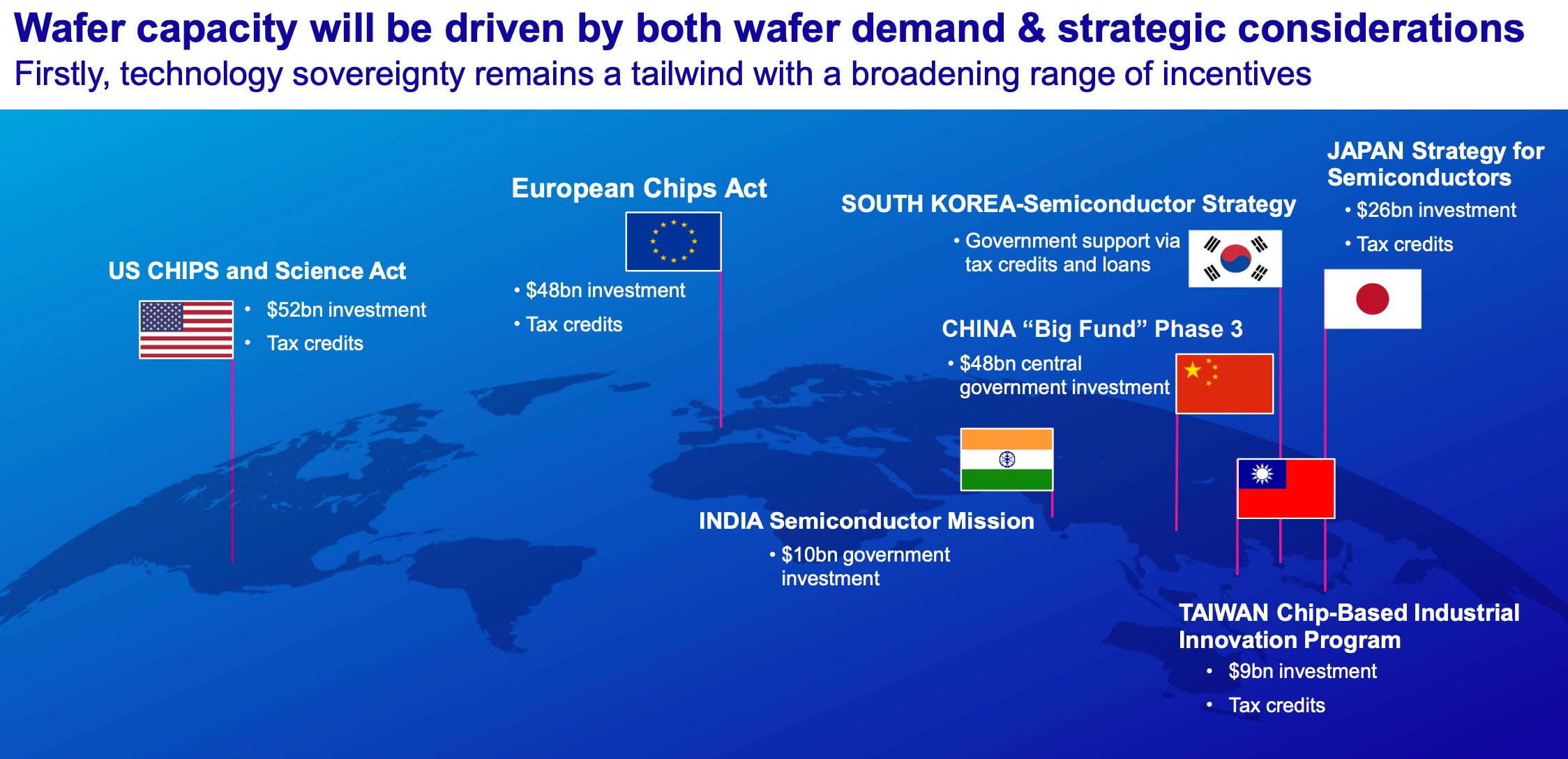
Upside longer term from potential sovereign investments (that could add 5-8% of extra capacity worldwide) for tech sovereignty and supply security reasons. Those could happen in US/EU/Korea/Japan to replace the ultra-dominance of Taiwan in advanced semiconductor manufacturing (>90% of advanced chips produced). For example, ASML has already received orders from Rapidus, a brand new leading edge foundry created in Japan, for its first fab (still in its early days).

Importance of ASP to ASML’s growth and system sales:
In 2023, ASML sold 600 systems, of which 75% came from lithography systems and 25% from Metrology & Inspection systems. Lithography systems have a significantly higher price points than M&I systems. The average lithography system is €47m (EUV low NA average price at €170m) while an M&I system average price is at €4m. Therefore, lithography contributes to 97% of the system sales in terms of € amount.
In lithography systems, the more leading edge the system, the higher the average price. The latest low-NA tool (the 3800) average sales price (ASP) is around €210m, the next low-NA tool (4000) with higher wafer productivity of 250wph is estimated to be €270m.
Risks & Threats
Heavy customer concentration: largest 2 customers represent 67% of sales and TSMC risks becoming a near monopoly on the foundry side, likely to lead to more volatility around order intake (which explains why the company will stop reporting on this metric quaterly from 2026 in favor for an annual number).
Worst-case scenario: only TSMC is leading the 2nm and below race, ASML litho pricing can stand as they reiterated their irreplaceable position as the only EUV provider in the world. They also believe that their value-based pricing is reasonable considering: 1) Resolution; 2) Overlay, 3) Productivity. In addition, TSMC has a much higher gross margin (>60%) than ASML (>50%). The company has also shown its willingness to stand firm when negotiating large contracts with TSMC, even if it means waiting a quarter or two to book the order (as has been the case for a large part of TSMC’s 2nm orders).
Key end demands area for 2nm chips is AI-driven high-performance computing (HPC) - server/datacenters.
Historically, smartphones have driven initial leading-edge node adoption, which was later followed by server computing with several years of lag.
However, now that Al has become the dominant growth driver within semis and the Big Tech giants have put in place capex plans to enhance their large language models, demands for high-performance chips are significantly increasing, and are estimated to overtake smartphones over next few years.
Uncertain customers' capex and technology adoption plans (still a cyclical industry). The 3 largest chip producers in the world have all announced plans for advancing into 2nm node chips production, in new fabs. These are important to monitor as their orders will be important catalysts for ASML.
TSMC: the production of 2nm chips (called N2) will be ready in H2 2025. The company will ramp N2 in 2 newly-built fabs based in Taiwan (Hsinchu and Kaohsiung) with additional capacity coming from two fabs in Arizona (Arizona fabs 2 and 3). The company has consistently reiterated that customer demand seems strong with a high level of customer engagement. For the moment, they disclosed that the performance and yield of N2 production is on track or ahead of plan.
Samsung: the production of 2nm chips (called SF2) is estimated to be ready in 2025 for mobile applications, in 2026 for high performance computing (HPC), and in 2027 for automotive applications. The ramp will likely come from newly-built 4/5 fabs in Pyeongtaek, South Korea. Samsung is still struggling with low yield rates in 3nm (some media reports at between 10-20%, vs TSMC 60%-70%). However, the company is reportedly ramping up its efforts for the mass production of 2nm and 1.4nm (aiming for 2027) to secure its advanced lead in the world.
Intel: the recent change in leadership (ex Cadence Design CEO is new Intel CEO), operational and financial struggles and pushout of fabs puts in doubt Intel’s capex plans. Profit warning + layoffs + dividend cut + capex cut announced in August 2024 (Q2 earnings): Intel announced that it 1) reduces opex (including R&D and SG&A) to $20bn in 2024 and $17.5bn in 2025, as well as laying off >15% people; 2) reduces capex by >20% in 2024 to $25-27bn and in 2025 to $20-23bn, Qualcomm has approached Intel for a potential buyout in September 2024.
Geopolitical tensions and regulatory risk: export control and China sales.
Since September 2024, the Dutch government is the one responsible for issuing export licenses for ASML’s exports of advanced semiconductor manufacturing equipment, for national security reasons.
ASML published a separate statement saying that the latest measures from the government mark a "technical change" that are not expected to have any impact on its financial outlook for 2024, or for-its longer-term scenario.
A reminder of ASML's system sales restrictions:
EUV - cannot be sold at all to Chinese firms since January 2020.
DUV - basically cannot sell more advanced DUV immersion systems to China since June 2023 + need to apply for export licenses with Dutch government for mature DUV.
3D stacking technology into logic chips and DRAM may reduce lithography intensity.
Focus of investor, given the shift this year with 2nm to GAA architecture (3D architecture of transistor) is on stacking technologies like those of ASMi and Besi.
Competition: Chinese efforts to develop lithography tools, even though they will take a long time to create DUV tools and upwards of 10-15 years for EUV so should not be an issue in the time frame that concerns investors. The combination of exceptionally high technological and supply chain barriers explains why ASML stands alone in the industry and will not be contested for many years to come.
ASML is the global leader in lithography. It maintains 90% of market share in lithography, 80% market share in DUV market and is the sole provider of EUV machines. Nikon (30% of revenue from semis) competes with ASML on ArFi (DUV) while Canon (7.5% of revenue from semis focuses on older technologies including KrF & - i/g line. Hard for new entrants & existing players to take up market share:
Phenomenal technological barriers: ASML has established a very broad and strong intellectual property portfolio, but still maintains the highest R&D/sales in the semicap industry (and has a 15 year roadmap for the upgrade of its EUV tools, ensuring it will remain essential for customers and will never be overtaken). ASML has 14% of sales on R&D vs Nikon 10% and Canon 8%. It's also the highest if we compare it to broader WFE players: Applied Materials 11%, Tokyo Electron 13% and Lam Research 13%.
Ecosystem & heavy capex barrier: the manufacturing of lithography machines requires a lot of knowhow from ASML, but also of from its many suppliers, partners and knowledge institutions. New entrants need significant efforts to understand the supply chain of different specialized parts and need costly and very complex investments to compete in this industry.
Recent profit warning:
ASML published its Q3 24 results 1 day earlier by accident. The profit warning: 1) narrowed down the 2025 sales guidance from prior €30-40bn to €30-35bn, which surprised the market as the management had a bullish tone during its 2022 CMD & Q1/Q2 2024, expecting the upper end of the 2025 guidance; 2) lowered 2025 gross margin target from prior 54-56% to 51-53%; 3) issued a warning that Q3 system bookings was €2.6bn vs €5.4bn consensus. Led to the stock price plunging by -16%.
Key reasons for the profit warning:
1) Customers capex cut/delay: while TSMC largely maintains its investment plan and is on track for its next edge technology (2nm), both Intel and Samsung have faced operational challenges to move to 2nm. As a result, they are pushing out (not necessarily cancelling) investments and plant additions, resulting in changes to demand timing, particularly for EUV (more profitable for ASML).
2) End markets are slower to recover than expected: key end markets for semiconductors are PC, phone, automobile, consumer electronics, industrials (including Life Science) and datacenters & servers. The demand in these end markets (except for AI) remains relatively low, and the recovery is also slower than expected. ASML noted that there continues to be strong developments and upside potential in AI-related demand.
3) China: ASML is now expecting China to be around 20% of revenue in 2025 vs 41% of 2024 revenues, indicating a 20%-30% YoY decline (as ASML’s overall revenue will still grow). While the market expected China sales to normalize, the drop to 20% of revenues (historical exposure) as soon as 2025 was more bearish than expected. This accelerated normalization is likely to be due to the very strong demand from Chinese customers in the last 2 years leading to inventory buildup, in a context of tightening export controls.
Financial Robustness & Capital Allocation
Stellar financial performance should continue (last 5 years: 24% revenue and 34% EPS CAGR):
ASML has had a very strong financial profile in the past, with a remarkable +24% revenue CAGR in last 5 years (driven by strong system sales growth: innovation/ASP + growth in client capex) and incredible EBIT margin expansion of 10pts in 10 years (from 23% in 2013 to 33% in 2023), while maintaining R&D / sales at the highest level in semicap industry at 14%. This has driven a 34% EPS CAGR over the last 5 years. In addition, it has a strong balance sheet with net cash position (€3.5bn net cash), with strong cash generation (average FCF/sales at 30% in last 5 years but has been volatile as the company gives favorable payment terms to its customers in a tougher environment) deriving from its high operating margin.
Going forward: near-term weakness in some end markets (smartphone, PC, auto) and pushout of some clients’ investments have impacted the stock (on top of the geopolitical climate and uncertainty around future export control as current impact has been very limited), but the company should be able to deliver a 10 year revenue CAGR of >10% with EBIT margin expanding to 43%.
Capital allocation: Focused investment in the business supported by a strong and flexible balance sheet
In the last decade, ASML has heavily invested in its organic growth through R&D (nearly quadrupled in a decade, ensuring its monopoly position in EUV will last well until the 2030s) and capex (capacity expansions to build the infrastructure for growth). The company has also made some strategic acquisitions to strengthen its supply chain (Carl Zeiss SMT, Berliner Glas).
The creation of new business (Metrology and Inspection with E Beam and Multi Beam) helped to accompany Moore's Law.
Spike in R&D in past couple of years. Also stepped up, capex to build infra to prepare for growth.
Since 2020, the company has accelerated the return of capital to shareholders. ASML has cumulatively returned nearly €40bn to its shareholders since its IPO.

Value creation: Shareholder return since 2010 23% vs 22% SOX and 17% NASDAQ.
In the last decade (and despite a difficult last year), ASML has outperformed both the NASDAQ (tech) and SOX (semiconductor) indexes.
This shows that its investments have payed off, delivering 18% systems revenue and 22% EPS growth CAGR over 2014-24 (4.5x 2014 revenue).
Gross margin improvements have also been impressive from 44% in 2014 to 51% in 2024. The drop since 2021 is linked to the ramp up in High NA EUV (impact more than 53% to 51% drop). €20bn in share buybacks explains the 22% EPS CAGR.


Outlook/Guidance
ASML delivered a stellar +20% growth on revenue from 2020 to 2024, driven by the secular technological trends of electrification and digitalization that drive up the demand for semiconductors, which according to Gartner, is expected to grow at +9% CAGR through 2030. ASML also benefits from customers' increasing adoption of leading-edge EUV lithography (with higher ASPs so higher revenue).
In 2024, the management announced an unprecedented profit warning that reduced its 2025 financial target mid-point, expecting revenue of €30-35bn (vs prior €30-40bn) and gross margin 51%-53% (vs. prior 54%-56%). The main reason is that its largest customers, including Intel and Samsung, have encountered issues in advance node manufacturing which disrupted their EUV adoption roadmap + the end demand is not picking up as expected. ASML maintained its 2030 target expecting top-line to be €44-60bn (mid-point representing +11% CAGR from 2024-2030) and gross margin to reach 56-60%.
2025 outlook (set in 2022) was downgraded at Q3 24: The company ended the year with 2024 revenues of €28bn and gross margin of 51.3%. For 2025, the disappointing part is that ASML maintained its guidance which was lowered, looking at group revenue €30-35b indicating +13% YoY in the mid-point, gross margin 51-53%. They reiterated that the main area of growth would be AI. The unchanged guidance is cautious given that regulation uncertainty is still there since Trump just started his term.
The company announced that it will no longer report quarterly order intake starting in 2026 but only communicate on an annual backlog number. This reduced disclosure could reduce the volatility around the earnings with a lumpy order intake detracting from the momentum of the business. This will align ASML with other large cap semi equipment vendors.
2024 CMD:
ASML delivered a confident message about its 2025-30 outlook and the opportunities it sees in semis (size and technology transition), the market welcomed the CMD and the stock price ended up by +7% on the day. The presentations focused on an updated view of the market up to 2030, ASML's roadmap to address this demand and meet the industry's challenges, with the company at the center of the industry's innovation roadmap and answer for Al challenges on cost and energy consumption, as well as its financial forecast.
Markets: ASML reiterated its view of a $1tn semiconductor market in 2030 but with a significant change in mix with AI compensating the weakness elsewhere. AI is playing a much bigger part (40% of the semi market by 2030) and driving growth in advanced logic (foundries) and DRAM (HBM memory, the bottleneck for AI), which is positive for lithography intensity. This change in mix in the market (more AI, less of the rest) explains in part the transition the market is going through (plus the weakness of other end markets) and explains the less bullish view for 2025, but the outlook remains very strong for 2030 with an increased need for EUV (management speaks about scalability for many generations).
By end markets: more growth from datacenters & servers, and less from other end markets notably phones, PC & automobile.
By chip type: more growth from advanced logic (10-20% litho CAGR 2025-30) and DRAM (15-25% CAGR), while lower growth from NAND and mainstream market.
By product: EUV (where ASML has 100% market share) will be the main growth engine +10-20% CAGR in advanced logic EUV litho spend, + 15-25% in DRAM. DUV (its more mature technology) will still see growth, from more wafers & more layers in mature and leading edge chips. Finally, its large installed base will continue to deliver growth (13% CAGR) from value based services and upgrades.
Financials: 2030 targets were left unchanged vs its CMD two years ago: revenue €44-60bn, mid-point €52bn indicates a +9% CAGR from 2023-2030, gross margin 56-60%, expenses €1bn higher on CAPEX (7% of revenue now) and €250m higher for SG&A. Management gave their underlying assumptions, which did not include a significant rebound in demand for phones, PC or other devices driven by gen-Al replacement cycle. Its datacenter market assumptions ($350bn in 2030) also look reasonable and are thus reassuring. Gross margin improvements are mainly from EUV with Low NA volume pickup and R&D roadmap (greater throughput so ASP and margin) and High NA closer to group margin. Volumes will also help in DUV and installed base business.

Governance & Management Quality
ASML has a very competent management team with all members having spent a significant amount of time with the company. New CEO/Chair Christophe Fouquet was promoted to CEO in 2024. After its unprecedented profit warning in Q3 24, for the first time in a long time, there are concerns about the management's credibility, which I think are unwarranted given the quality and track record of the management.
CEO Christophe Fouquet joined ASML in 2008 and has served a broad range of leadership roles (most notably in charge of the EUV business, successfully developing and rolling out ASML’s most important product) being promoted to group CEO replacing his predecessor Peter Wennink that left for retirement in 2024, most recently as Chief Business Officer, and previously as EVP EUV. Prior to joining ASML, he worked at KLA Tencor and Applied Materials.
CFO Roger Dassen joined ASML in 2018 as group CFO. Prior to joining ASML, he worked at Deloitte Touche Tomatsu Ltd as global Vice Chair and member of the executive board. Previously he was CEO of Deloitte Holding BV (2005-2012) and Audit Partner at Deloitte Netherlands (1996-2018).
Shareholders: ASML has no controlling shareholders (59% institutional investors and 41% public investors), the top 5 shareholders represent 20% of shares. Largest individual shareholders are: the prior CEO who just retired Peter Wennink, owning 0.01% shares (market value $35m), and current COO Frederic Schneider-Maunoury, owning 0.01% shares (market value $18m).
Remuneration: Strong alignment of management with shareholders. CEO has €1m base pay, short term incentives (max 120% of base) linked to EBIT margin (60%), technology leadership of company (20%) and customer orientation/internal projects (20%), long term incentives (shares based, max 200% of base) linked to TSR (30%), ROIC (40%), tech leadership (20%) and sustainability (10%).
Valuation
The recent weakness provides an attractive opportunity for a company that has very rare visibility into the demand for its product (embedded in their customers' roadmaps for the next decade and are the key driver for the digitalisation of the world: AI, smartphone, IoT etc), huge barriers to entry and ultra dominant in its market and with strong long-term demand growth coming for semiconductors driven by continuing electrification & digitalization which is currently impacted by weak macro economy, but not structural.
The bottom line is that ASML’s EPS should grow x2.5 from >€20 in 2024 to >€50 in 2030, making it a great company to own for the next 3-5 years and beyond.
Upside from rerating: The company is trading at 21x 2025 EBITDA vs a historical average of 27x EBITDA, giving a 25% upside if it comes back to its historical multiple. This only underwrites the low end of the company's 2030 guidance with back-end loaded the growth: meaning revenue growth of 6.5% over 2025-30, only equal to the growth in wafer demand vs between 6.5-13% CAGR forecasted by the company given the strong growth in EUV demand from DRAM and advanced logic during the period, in part due to Al, and consistent with the investment needs in memory and at TSMC linked to semiconductor growth.
Bear case: the geopolitical tensions and weakening macro environment could impact the company’s outlook for this year and delay the rerating. But the operational issues at their customers are already built into the guidance and the demand from AI remains strong as seen in TSMC’s huge capex guidance for 2025.
Catalysts:
A major catalyst for the sector and ASML will be when the company gives more colour on its 2026 expected growth (for now the company has only indicated that it will be a growth year).
Higher than expected revenues from China (as a reminder the company is expecting -30% yoy decline) this year could help ASML mitigate capex uncertainty at other clients.
DRAM spend (linked to HBM memory used in AI data centers) could also suprise positively this year and going forward.
Disclaimer: The information provided on this Substack is for general informational and educational purposes only, and should not be construed as investment advice. Nothing produced here should be considered a recommendation to buy or sell any particular security.