
Optical & Networking Supercycle at the Heart of the AI Revolution
The AI networking and optical supercycle, spanning hyperscaler capex, data‑center architectures, copper and optical connectivity, silicon photonics, and co‑packaged optics


Along with my friend Nick Nemeth from Mispriced Assets, we are releasing the most comprehensive deep dive yet on the Optical & Networking supercycle at the heart of the AI revolution. As the industry shifts from the training‑heavy GPU boom to the Age of Inference, the bottleneck is no longer just compute, it is the nervous system that moves data between chips at scale.
Every hyperscaler is now vertically integrating, designing custom networking silicon, optical engines, and full-stack interconnect fabrics, to claw back economics, reduce dependence on Nvidia, and break its chokehold on AI infrastructure. This report maps that power shift: from copper to photons, from pluggables to co‑packaged optics, and from legacy OEMs to the new optical and networking champions that will define the next decade of AI data center value creation.
Twice a week, I will release deep dives into stocks and sectors that fit into the three themes that I see winning in this age of tariffs and deglobalization: resilience, sovereignty & reshoring, China. I will then deep dive into the opportunities in the AI data center value chain, healthcare and much more.
Take advantage of this once in a generation opportunity to build long term wealth by investing in great stocks that will deliver returns for your portfolio for years to come.
Before this deep dive, I recommend reading some of our other write ups on the AI data center megatrend:
Understand how to invest in the $3-4tn AI Supercycle, a once in a lifetime investment opportunity.

To understand the structure of the ecosystem, read this primer on the AI data center buildout.

The AI revolution is all about semiconductors. Enjoy the most comprehensive deep dive into semiconductors, the most important sector in the world, and it’s completely free! Listen to the podcast or read the article to become an expert on semiconductors and understand the big trends from AI to semi production, fabless companies to equipment makers.

Discover one of the defining megatrends of our generation, the coming boom in electricity demand and grid investment supercycle, and how to play this decade long structural opportunity. This megatrend is completely intertwined with the AI data center buildout, making it crucial to understand Electrification.

The Age of Copper: Riding the Electrification, AI Data Center and Grid Investment Supercycles: Understand why copper is uniquely positioned at the heart of the electrification and AI data center supercycles, what is means for the metal’s price and how to get exposure to copper

Coherent vs Lumentum: The tale of the 2 optical networking champions
Understand Coherent, the optical leader, with Nick’s excellent deep dive from Aug 2025

Table of content
Why is everyone talking about AI networking and Optical names?
Who are the players?
The Revised Thesis: The US Optical Duopoly and the CPO Reality Check
Why is AI networking the next bottleneck?
AI Networking and Scale Up vs Scale Out
Market Dynamics: A Networking and Optical Supercycle
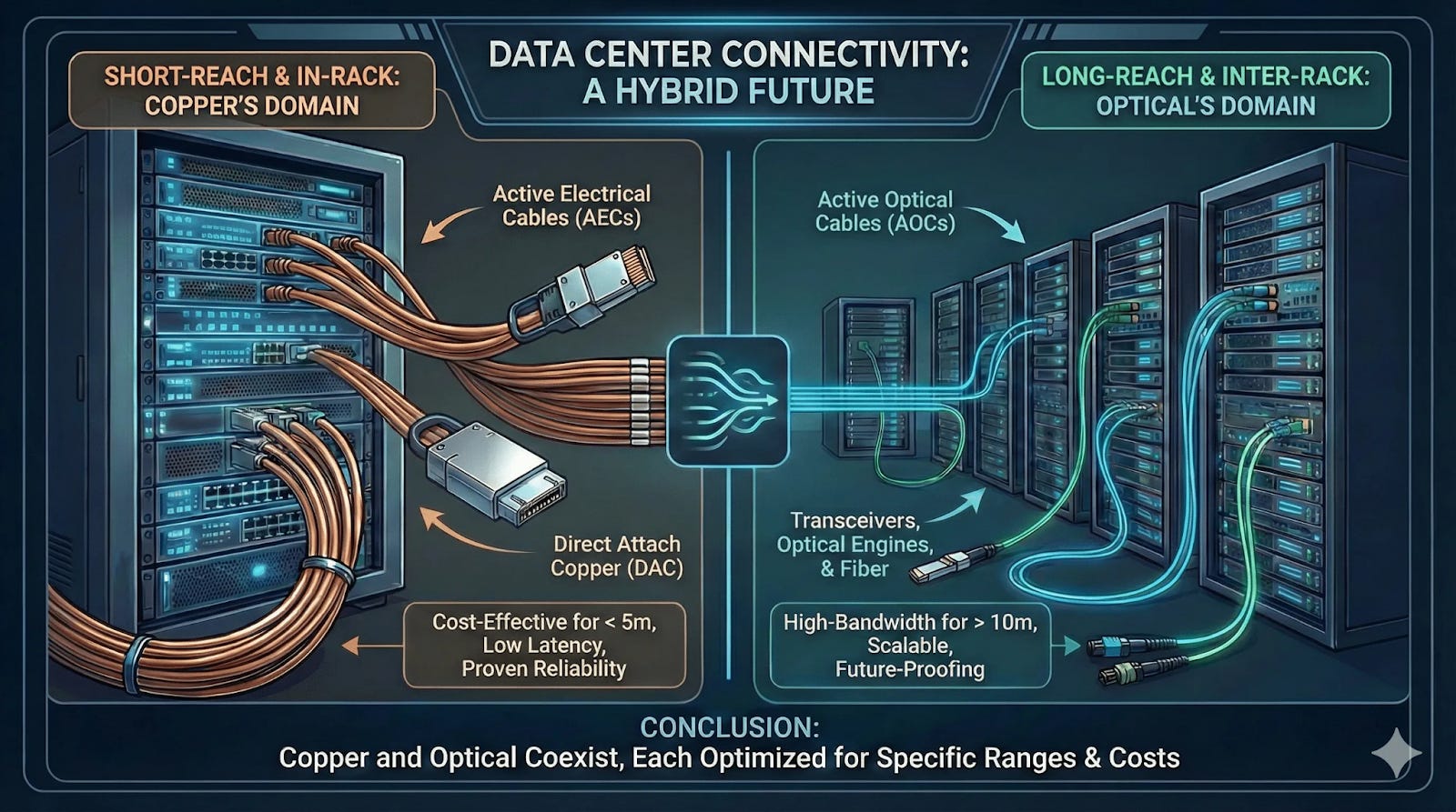
Copper Connectivity in Data Centers
Optical Connectivity in Data Centers
What is Optical Connectivity? The Technical Analysis
The Rise of Silicon Photonics
Optical Circuit Switching: MEMS vs. Liquid Crystal
CPO: The Future of Optical Connectivity
Why is everyone talking about Optical and Networking names all of a sudden?
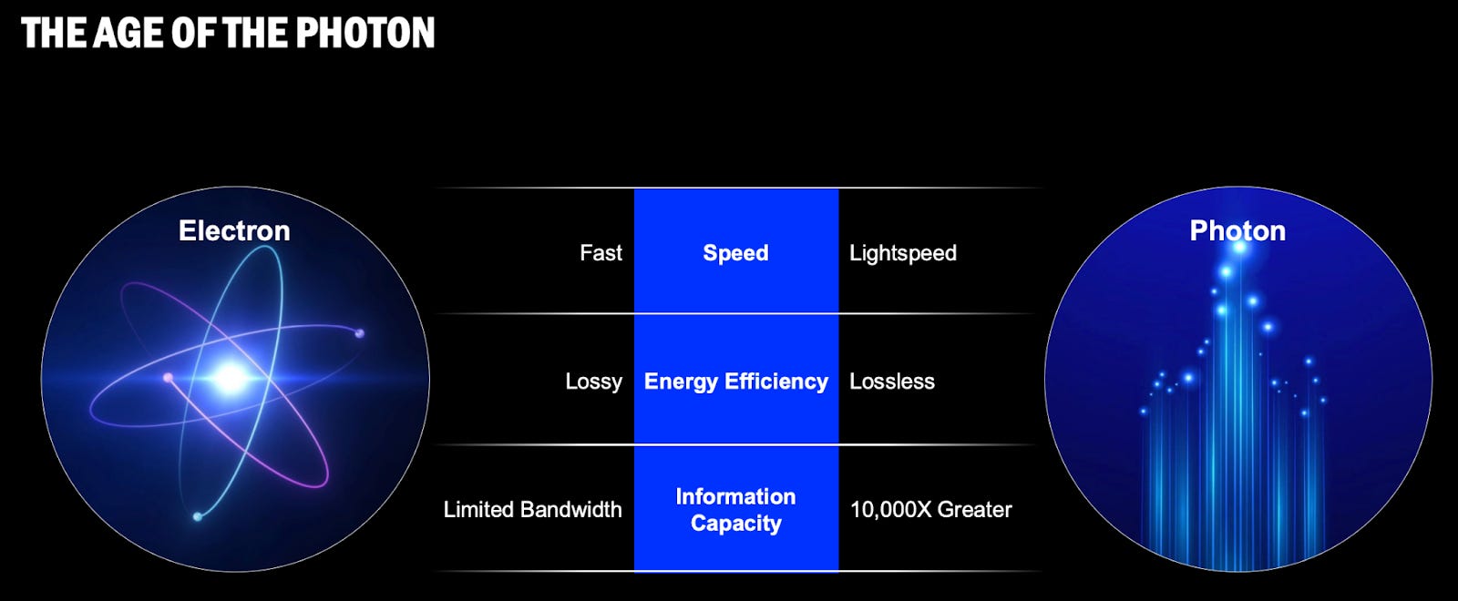
Copper, which we have used to power our communications for centuries, has hit a physical wall. As the AI supercycle accelerates, moving data is now all about moving photons and not electrons and the companies mastering the optical world are at the heart of the AI ecosystem. Why? Photons go at lightspeed, are extremely energy efficient and can carry a gigantic amount of information.
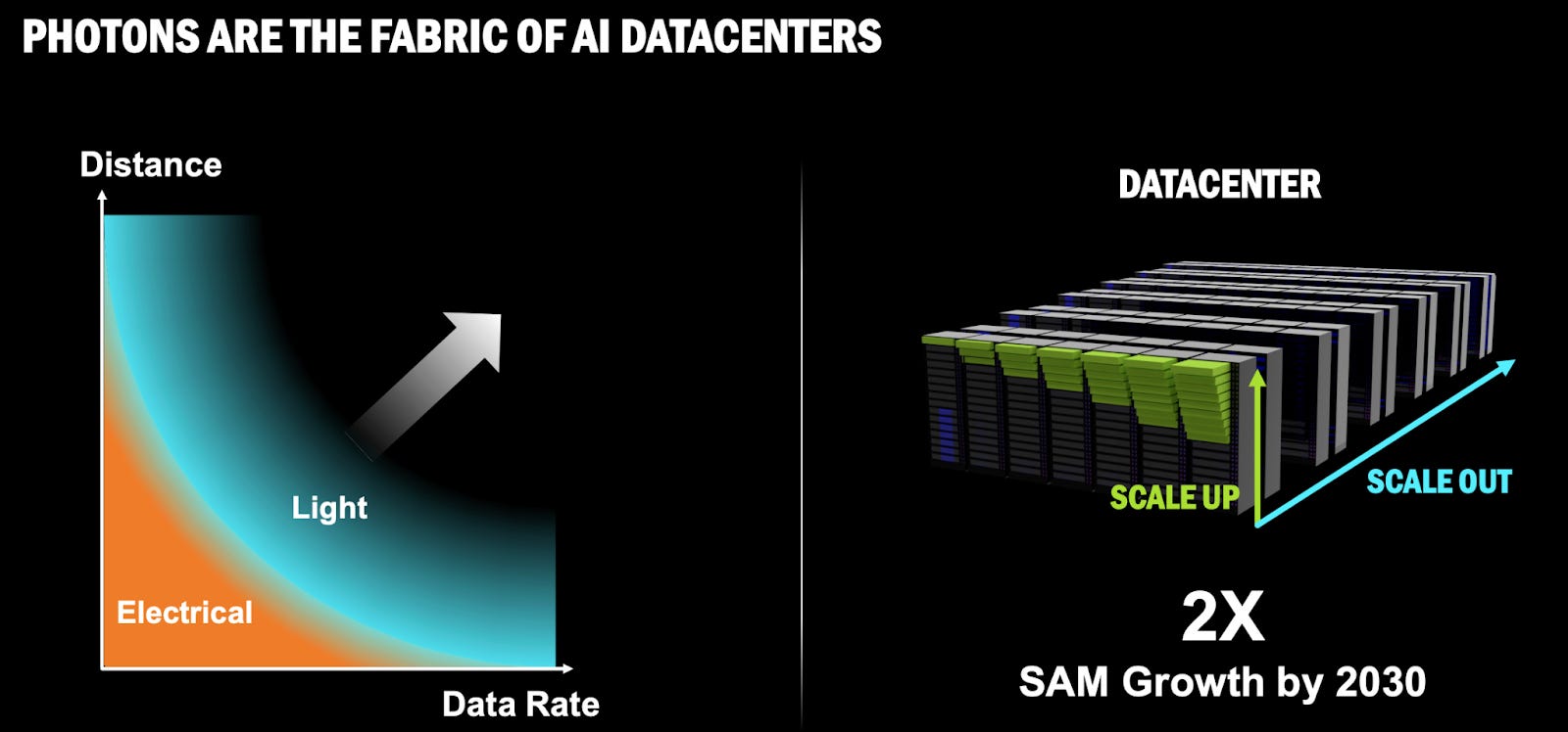
The conversation is shifting from the brain (GPUs like Nvidia’s H100) to the nervous system (networking). While computing power has grown exponentially, the ability to move data between those chips has become the primary bottleneck. We are currently hitting a physical wall known as the E-O Divide (Electrical to Optical). As data rates exceed 100 Gbps, copper cables (electrical) physically cannot carry signals further than a few meters without the signal degrading into noise or the cable acting as a heater. Consequently, the industry is forced to switch from copper to optical (light-based) interconnects at shorter and shorter distances, effectively creating a massive new hardware market inside the data center
AI data centers drive upgrade cycle of networking industry:
AI computing is fundamentally rewiring networking needs: In the past, systems were primarily based on retrieval-based computing, where the content was pre-built by others and then delivered. Now, the shift is toward generative-based computing, in which software generates unique content in real time based on context, scenarios, and prompts. Due to the real-time and unique nature of generative content, the global demand is emerging for AI factories that can produce content instantly. Cloud and AI infrastructure are entering a period of rapid expansion.
Overall capex is expected to maintain high growth momentum in the coming years, benefiting networking: Hyperscalers just keep increasing their investments into AI data centers, which could reach $550bn in 2026, 4-5% of which goes towards connectivity.
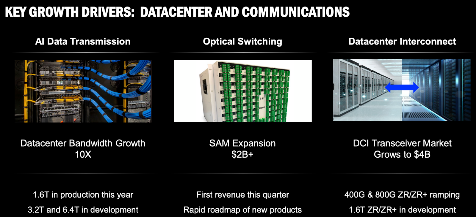
800G optical transceiver shipment to double: The optical communication segment has benefited from the ramp up of Nvidia’s Blackwell and Rubin platforms and the continuous upward revision of AI data center capex which is accelerating the transition of network transmission speeds toward 800G and 1.6T. The ramp of the 800G optical transceiver modules will begin in 2025-26, with demand expected to reach 40m units in 2026. Adoption of 1.6T modules is expected to begin in end-2025, with demand expected to exceed 20m units in 2026. These components are expected to deliver multiple-fold growth compared to 2025, which confirms that AI will continue to be the main driver of market growth between 2026 and 2030. Currently, continuous wave (CW) lasers and electro-absorption modulated lasers (EMLs) are falling short of demand.
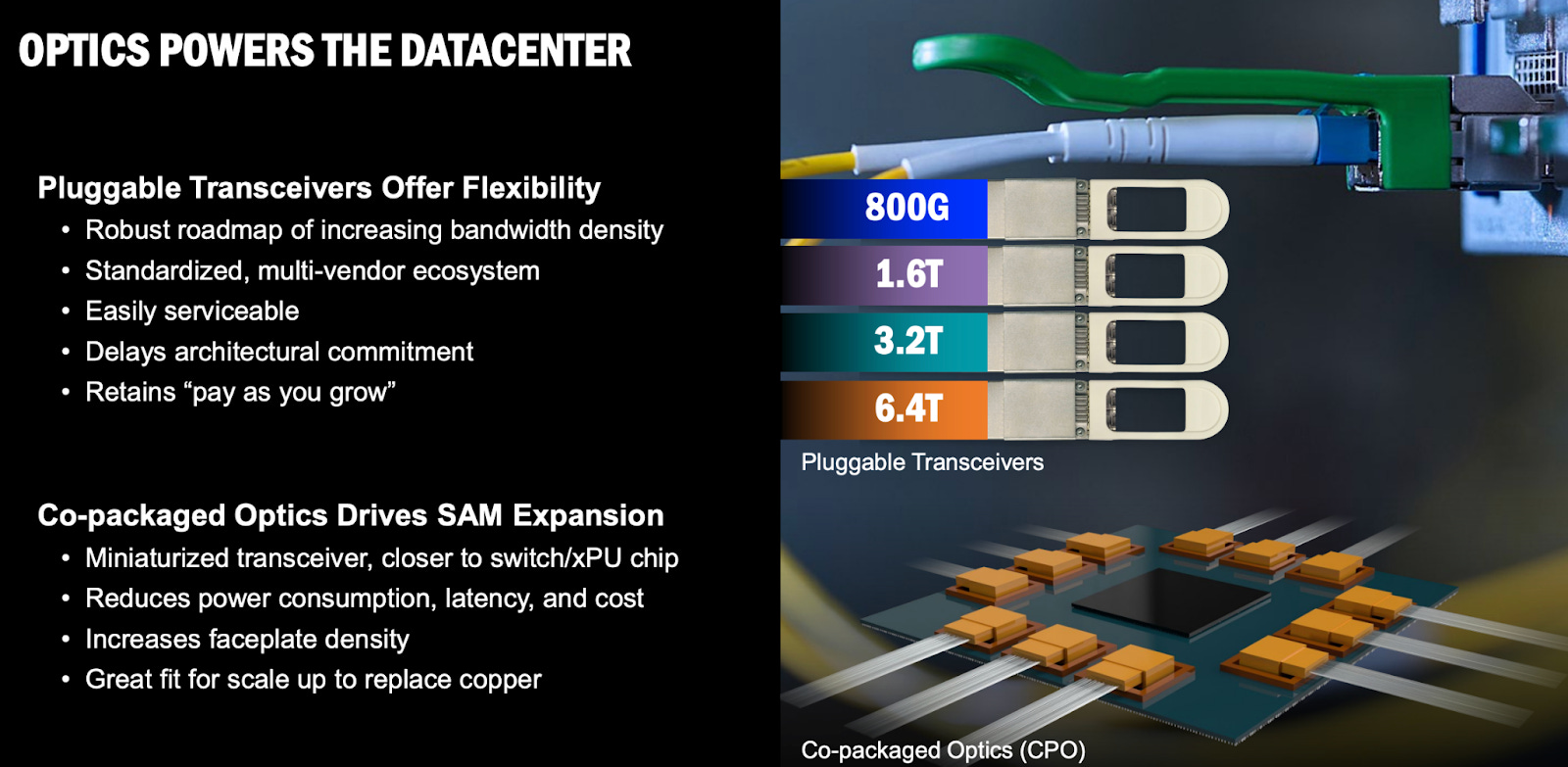
CPO poised for explosive growth: As data center’s requirements for bandwidth, low latency, and energy efficiency continue to rise, traditional pluggable optical modules and copper interconnects are reaching physical limits and can no longer fully meet the requirements of next-generation HPC and AI clusters. CPO is designed to address the bottlenecks of traditional solutions, specifically concerning power consumption, bandwidth, latency, and density. AI-driven workloads are the main catalyst for CPO adoption. CPO integrates the optical engines (OE) directly with the electronic chips such as the switch ASIC or processing units, auxiliary processing unit (XPUs) within the same package. This process aims to bring the optoelectronic conversion process as close as possible to the core silicon chips, thereby achieving higher transmission speeds and energy efficiency. For example, CPO reduces power consumption at 1.6T bandwidth from about 30W in traditional pluggable modules to about 9W. According to the roadmaps of major vendors and our discussions with component vendors, CPO will first be adopted in switches. The ASP of optical communication devices is expected to grow several folds after switches adopt CPO. Based on the current timeline, CPO could take off in H2 2026.
Networking/Optical names were all previously boring hardware companies that were not in broad portfolios as they were very cyclical and slow growing in the mid-single digits percent range, with down years up to -20% and up years above +25%. Margins were also low and quite volatile. They are now going through a structural shift higher due to Al with 2026 growth is expected between +17-77%. Corning was founded in 1936, Ciena 1992, Celestica 1994, but Lumentum 2015. These names have been very strong performers since mid-2024.
Why these companies are powerful AI data center plays:
They all involve networking and communication within a data center, which has room for growth as companies are all looking to move data faster.
The faster you can move data, the more efficient an entire system becomes, and therefore a faster ROI.
META has reported data spends 20-60% of the time moving around a data center instead of being processed.
Increasing network speeds by 20% can reduce the cost to train a leading model by 10-15%.
Networking is about 15% of AI capex (4-5% of capex for connectivity):
Of every $100 spent on AI clusters, the vast majority (think about 80%+) is spent on AI compute (GPU/ASIC) with around 15% dedicated to networking, spread across switches, network interface cards (NICs) and connectivity.
AI Ethernet Transceivers could jump 67% yoy to over $8.5bn 2025 and grow at a 26% CAGR towards $20bn+ by 2030, representing around 4-5% of total AI spend.
Pluggable optical modules, called transceivers, provide the fastest speeds/operational flexibility, but require expensive and power-hungry components.
Copper connectivity is cheaper but has speed/distance limitations.
CPO is currently unproven at-scale and can add operational complications.
What to monitor - optical and networking value capture moving from OEMs to semi makers?
Due to the AI wave and data center’s increasing demand for high speed and low power consumption, the explosive growth in internet traffic is driving spec upgrades of network communication equipment. As the deployment of silicon photonics and CPO technologies has become critical, TSMC’s Compact Universal Photonic Engine (COUPE) can meet a wide range of applications in terms of performance, power efficiency, and cost. Overall power consumption is expected to be reduced by more than 10x, while transmission efficiency could improve by 20x.
Future business opportunities could be focused on the key segments consisted of electronic integrated circuit (EIC), photonic integrated circuit (PIC) chip design and fabrication, advanced packaging and optoelectronic signal measurement of EIC and PIC, lasers, micro-lenses, optical coupling, FAU design, and optical adhesives. The related supply chain including optical communication components, III V epi, test interfaces, and equipment should benefit from the shift to silicon photonics and CPO.
Who are the players?
The supply chain is vast, with some of the most innovative companies in the world:
The Brains (DSP & Switch ASICs): These companies design the chips that direct traffic and process signals:
Broadcom & Marvell: They hold a near-duopoly on the Digital Signal Processor (DSP) chips inside optical modules and the Switch ASICs (like Tomahawk 5) that run the network.
Nvidia: Dominates the end-to-end system with its InfiniBand and Spectrum-X Ethernet switches.
The Module Makers (Transceivers): They assemble the lasers, DSPs, and optics into the pluggable units (silver sticks) you see in data centers.
Innolight & Eoptolink: The volume leaders, particularly for 800G and 1.6T transceivers.
Coherent & Lumentum: Major US-based players who also manufacture their own laser chips (vertical integration).
The Equipment Builders (Switches & Systems):
Arista Networks: The leader in Ethernet switching for hyperscalers (Meta/Microsoft).
Cisco & Dell: Traditional enterprise networking giants pivoting to AI infrastructure.
The Assemblers (Manufacturing):
Fabrinet: The manufacturing partner of choice for Nvidia and many western optical companies.
Celestica: Engineering-focused ODM, acts as a critical manufacturing partner for hyperscalers (most notably Google).
The Foundries (Advanced Chip Making):
TSMC: Critical for the next generation of Silicon Photonics and Co-Packaged Optics (CPO) via their COUPE platform.
The Difference: Networking vs. Optics
While often grouped together, these serve distinct physical functions in the data center. The simplest analogy is that Networking acts as the Traffic Cop (logic and routing), while Optics acts as the Highway (physical transport).
Networking (The Brains - Electrons): This refers to the switching and routing logic that directs data packets to their destination.
Core Hardware: Switch ASICs (Application-Specific Integrated Circuits). These are high-performance silicon chips (like Broadcom’s Tomahawk or Nvidia’s Spectrum) that process electrical signals to route data.
Protocols: The language spoken by the network. The current battle is between InfiniBand (proprietary, low latency, dominated by Nvidia) and Ethernet (open standard, dominated by Arista/Broadcom). Ethernet is currently gaining market share for backend AI networks due to cost and interoperability.
Optics (The Nerves - Photons): This refers to the physical medium used to transport data when the distance is too great for copper cables.
Core Hardware: Optical Transceivers (the “silver sticks” plugged into switches). These modules convert electrical signals from the switch into light (photons), send them down a fiber optic cable, and convert them back to electricity at the other end.
The E-O Divide: This is the boundary where physics dictates a switch from electricity (copper) to light. As data rates rise (to 100Gbps+), copper cables act as resistors/heaters and cannot transmit data further than 2-3 meters. Therefore, optics are required for any connection longer than a few meters, a threshold that is shrinking as speeds increase.
The Optical Companies:
Corning (GLW): $95bn market cap, $16.4bn revenues, 35-40% AI exposure, main products Optical Fiber, $25bn TAM, 25% market share, main customers Apple/Samsung (5% revenues each).
Ciena (CIEN): $34bn market cap, $4.8bn revenues, 35-40% AI exposure, main products Optical Communication Management, $20-22bn TAM, 10% market share, main customers 26% from 3 telecom companies.
Lumentum (LITE): $26bn market cap, $1.6bn revenues, >50% AI exposure, main products EML chips/Lasers/CPO, $20bn TAM, 10-20% market share, main customers 17% Google and 15% Ciena.
Celestica (CLS): $38bn market cap, $9.6bn revenues, 55-70% AI exposure, main products ASIC servers/White box switches, $100bn servers + $10bn switches TAM, 30% switches market share, main customers Google and Amazon 45% total.
Corning:
Corning is a material sciences company that makes glass and ceramic products for a variety of end markets Produce passive materials and components for optical fiber, cable, and connectors - the glass and cabling inside and between data centers and telecom networks is the AI exposure.
Six segments:
Display Tech (23%) - Glass monitors and phone screens
Optical Communications (41%) - Optical fiber and cable for networks/Al
Environmental Tech (11%) - Filter products for autos to reduce emissions
Specialty Materials (14%) - Highly durable products like Gorilla Glass, specialty optical, semi packaging
Life Sciences (6%) - Lab equipment consumables
Emerging growth (9%) - New growth areas like Hemlock semis and poly silicon
13% growth in 2026, 13% in 2027 and 12% in 2028.
Glass is only solution for applications like optical signal transmission, etching electronics on transparencies
Geographic breakdown: Asia is 50% with 33% is China, North America 36%, Germany 11%
No significant competitors in the US, no close public peers, but small peers in individual segments
Ciena:
Sell the entire optical networking system to clients further up the stack. Optical transceivers, optical transport systems, switching platforms, network management software
4 segments but end revenue is broken down into 3 areas:
Optical network systems (67%) - transport, packet switching, interconnect platforms, optics
Routers and switches (10%)
Support and service (22%)
24% growth in 2026, 17% in 2027 and 13% in 2028.
Does not design its own silicon but buys silicon from companies like Broadcom and combines them with its own photonics.
Number 1 market share in hyperscale data centers and optical transport, as well as service provider optical transport
Geographic breakdown: Americas 74%, EMEA 16%, APAC 10%
Competitors: Huawei, JNPR, CSCO, ZTE, Nokia
Corning provides the optical fiber for Ciena’s networking equipment, have been partners for a long time.
Lumentum:
Designer and manufacturer of optical and photonic products:
Essential to a range of cloud, Al/ML, telecommunications, consumer, and industrial end-market application
Lasers used for data transmission between GPUs, CPUs, switches in Al clusters
Optical transceivers, pump lasers for DCI and long haul fiber optic links, optical circuit switches
CPO and indium phosphate chips that transition DCs from copper to photonics
Support access (local), metro (intracity, long-haul (intercity and global), and submarine (undersea) network infrastructure
2 segments:
Cloud Networking (85%) - optical communications
Industrial tech (15%) - lasers for 3D sensing, Lidar, fiber
60% growth in 2026, 40% in 2027 and 25% in 2028.
Lumentum and Ciena have a strategic partnership where Ciena supplies the technology and LITE is the manufacturing and distribution partner along with supplying components.
Is working with Nvidia on advanced networking tech for AI infrastructure.
Geographic breakdown: APAC 61%, Americas 29%, EMEA 10%
Competitors: Ciena, Coherent, IPG Photonics
The Revised Thesis: The US Optical Duopoly and the CPO Reality Check
The “one winner” take in AI optics misses the real constraint: supply. HBM is gating server shipments, so hyperscalers are increasingly ordering networking and optics ahead of compute, and in some cases stocking modules so clusters can light up the moment GPUs arrive. In that world, two U.S. incumbents can win at the same time, just in different layers of the stack.
1. The Manufacturing Winner: Coherent (The Scale King)
Coherent reads like “legacy optics” until you look at the datacom factory: it’s built to ship volume, and volume is the product when demand is oversubscribed.
• The 6‑inch InP advantage: Coherent has disclosed its transition to 6‑inch InP wafer production (Texas + Sweden), which increases die per wafer meaningfully versus 3‑inch and improves unit economics when yields cooperate.
• Volume and pricing: In a shortage, the supplier that can ramp dependable output earns leverage. Pricing power exists, but realized margin depends on mix, contracts, and yield.
• Bottom line: Coherent is positioned for the “now” cycle, 800G/1.6T pluggables at scale, while the industry waits for CPO to graduate from pilots to fleets.
2. The Innovation Winner: Lumentum (Early Leader in High‑Power Lasers)
Lumentum’s edge is less about “more optics” and more about the hardest physics: high‑performance EMLs today and ultra‑high‑power external lasers that make first‑gen CPO architectures workable.
EML leadership: Lumentum is a key supplier of EMLs used across 800G/1.6T links, though share varies by customer and platform.
External Laser Source (ELS) for CPO: By moving the laser off the hot switch/GPU package and into a serviceable front‑panel module, ELS architectures address the thermal and maintenance constraints that break “laser‑on‑package” in practice. Ultra‑high‑power output helps overcome coupling and distribution loss.
“Monopoly” caveat: The right framing is “early volume leader in UHP/ELS,” not a permanent monopoly, competition is likely; timing is the variable.
Optics (CPO)
CPO is the direction of travel, but adoption is a product decision, not a physics proof: operators care about MTTR, blast radius, and upgrade flexibility.
Why CPO is “Amazing” (Physics)
Solving the copper/PCB wall: At very high speeds, you run out of electrical reach and equalization budget. Putting the optical engine on‑package shortens the electrical path and can remove or shrink DSP requirements.
Power/latency: CPO can cut module power and latency versus DSP‑heavy pluggables, but the delta depends on architecture (pluggable vs LPO/LRO vs CPO), switch design, and thermals, use ranges, not a single magic %.
The “But…” (Scaling, Reliability, and Maintenance)
Serviceability: Pluggables fail gracefully, you swap the module. CPO can fail with a larger blast radius, one bad component can take out many ports or force replacement of expensive assemblies. That’s the gating item for fleet rollouts.
Heat, and why external lasers matter: Lasers hate heat; GPUs and switch ASICs make heat. External lasers keep the light source in a cooler, serviceable location and feed the package over fiber.
Reach caveat (important): Near‑term CPO is primarily a scale‑out, rack‑to‑rack / switch‑to‑switch solution inside the data center. It doesn’t replace long‑reach links (campus/metro/telecom) and it doesn’t eliminate pluggables in the next 2–3 years.
Conclusion: You don’t have to pick one. Coherent is the capacity and cost‑down story for the pluggable build‑out that’s happening right now. Lumentum is the UHP/ELS optionality for when CPO ramps meaningfully. My take (and the part people miss): own the volume today, and keep a call option on the physics tomorrow.
Celestica:
Based in Canada, manufacturing company offering product design, engineering, manufacturing, testing, and supply chain/logistics across IT, A&D, healthcare, and industrials.
2 segments:
Connectivity and Cloud Solutions (72%) - compute, networking, storage for hyperscalers and enterprises
Advanced Technology Solutions (28%) - electronic products across industrial markets - very cyclical
34% growth in 2026, 35% in 2027 and 23% in 2028.
Compute revenue primarily derived from white box switches and custom ASIC servers.
Electronic Manufacturing Services is the core business where they manufacture to the design of the OEM, but the Original Device Manufacturing business is the growth area where they handle some of the design and manufacturing, then sell to others to be branded.
Hyperscale revenue has grown 50% CAGR over last few years: Google is 31% and Amazon is 14% of sales
Geographic breakdown: APAC 70%, Americas 20%
Competitors: Flex, Jabil, Accton, Quanta
Why is AI networking the next bottleneck?
The AI infrastructure buildout is rapidly accelerating as we move into the Age of Inference and AI adoption broadens throughout the entire economy. Capital is being allocated to hard assets at scale: data centers, networking infrastructure, power, cooling, and physical connectivity. For investors, the relevant question is no longer whether AI adoption continues, but where incremental capital earns excess returns that have not already been fully priced.
The bottleneck is caused by a fundamental shift in traffic patterns from Retrieval to Generative computing:
Old Era (North-South Traffic): In the cloud era (like with Netflix), a user requests a file, and the server sends it. Traffic flows out of the data center.
AI Era (East-West Traffic): In AI training, thousands of GPUs function as a single giant brain. They must constantly exchange parameters with each other to learn. This creates massive East-West traffic inside the data center.
The All-Reduce Problem: During training, every GPU must synchronize with every other GPU every few milliseconds. If the network is slow, expensive GPUs sit idle, burning money while waiting for data. This makes the network the governor on the engine of AI.
The Shift in Bottlenecks:
In the prior phase of the cycle, the dominant bottleneck was compute. The trade was straightforward: GPUs, Nvidia, and the hyperscalers. That trade worked because compute scarcity constrained AI deployment. That constraint has now moved.
As compute availability scaled, the system-level bottleneck migrated to data movement, specifically, networking bandwidth and latency inside AI clusters. GPUs today are increasingly underutilized due to data starvation, not compute limits.
The relevant framing is no longer the brain of AI systems, but the nervous system, the networks that connect tens of thousands of processors in real time.
Optical Transceivers:
Optical transceivers are a growing line item in server cluster bills of materials. Superficially, they resemble simple pluggable modules. In reality, they represent some of the most complex engineering within the data center.
Each module contains two primary components: the transmitter optical sub‑assembly (TOSSA) and the receiver optical sub‑assembly (ROSA). The TOSSA converts electrical signals into light via high‑powered lasers operating at extremely high frequencies (we are talking about billions of times a second). Then the light travels through an optical cable and the ROSA at the other end converts incoming photons back into electrical signals. These processes must operate flawlessly in high‑temperature, high‑density environments with zero tolerance for error.
The Electrical-to-Optical (E-O) Divide:
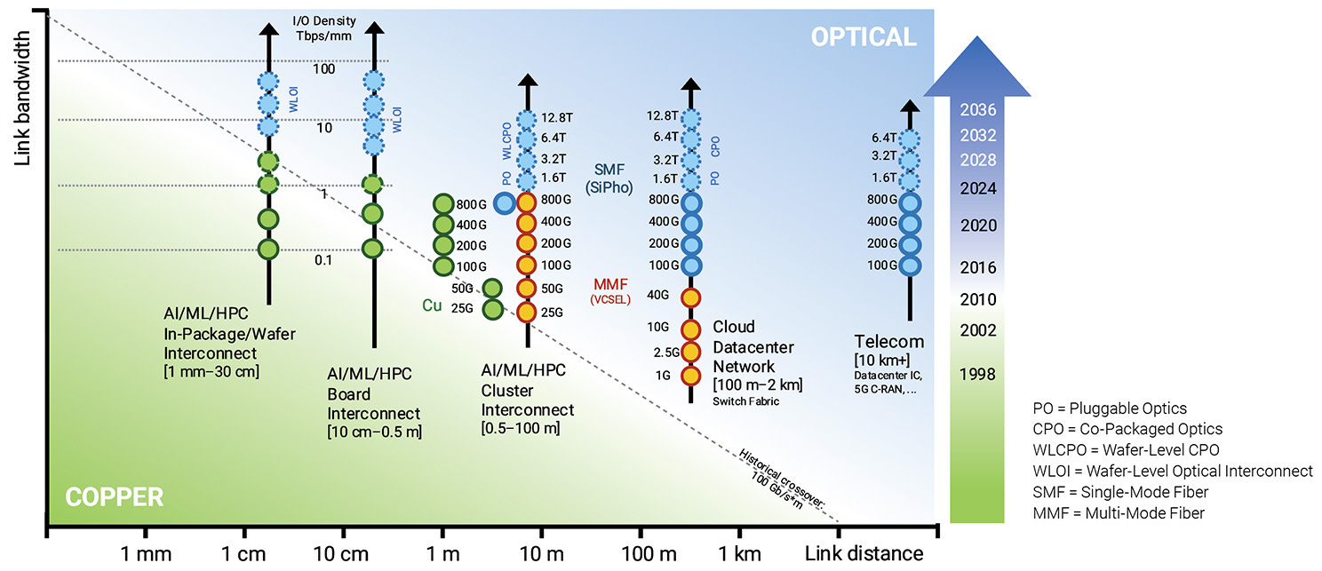
Replacement of copper by fiber/optical driven by bandwidth requirements. While historically the adoption of optical was reserved to transmit a signal several thousand kilometers across a continent, as opposed to a few hundred meters across a datacenter, there has been increasing adoption at shorter distances, given the strong appetite for higher bandwidth (100G, 400G, 800G) coupled with the need to reduce cost per bit and power consumption.
But even more importantly, at the center of this transition is the electrical-to-optical (E-O) divide (seen below), a hard physical limit that now dictates infrastructure design and capital allocation.
Copper interconnects face two non-negotiable constraints:
Heat generation due to resistance
Signal degradation at high frequencies (skin effect and insertion loss): at high frequencies, electrons that flowed normally through the whole wire are pushed to the edges (skin of the wire) due to the alternative current and this then creates immense heat as frequency rises
At modern data rates, 100G to 200G per lane, copper becomes impractical beyond approximately two meters. At these speeds, copper effectively functions as a heating element, not a transmission medium.
Historically, optical interconnects were used for long-haul communication. Inside data centers, copper was sufficient. That distinction has collapsed. The E-O divide is now inside the data center, and in many cases inside a single server rack.
This forces a structural shift from copper to optical connectivity, even for short-reach applications. The economic consequence is significant: replacing low-cost copper cables with high-value optical modules at massive unit volumes.
Why This Is Occurring Now - Generative AI Architecture:
The immediate catalyst is not AI broadly, but generative AI architecture.
Web 2.0 systems were retrieval-based. Data was stored statically and delivered primarily via north–south traffic (server to user). Server-to-server communication was limited.
Generative AI inverts this model. Training large models requires thousands, often tens of thousands, of GPUs operating as a single distributed system. Each GPU holds a portion of the model and must synchronize continuously with all others through operations such as all-reduce.
This creates extreme east–west traffic inside the data center, characterized by bursty, all-to-all communication patterns. Network performance directly determines GPU utilization.
At current GPU economics, idle time translates directly into cash burn. The network is now the governor on AI system efficiency.
Optical Attach Rates and Non-Linear Growth:
The key variable for investors is the optical attach rate, the number of high-speed optical transceivers required per GPU.
This ratio has changed structurally:
Early deep learning systems operated at roughly 1:1
Modern large-scale AI clusters operate at 3:1
Next-generation architectures are projected to approach 5:1
As clusters scale, network complexity grows faster than node count. Optical demand therefore grows super-linearly relative to GPU shipments.
This dynamic explains the magnitude of recent total addressable market revisions. The optical networking TAM is growing very rapidly, reflecting recognition of both scale-out (more GPUs) and scale-up (more connectivity per GPU).
Current and Emerging Technology Standards:
800G is the dominant deployment standard in 2026. Hyperscalers are rolling this out at scale using white-box networking architectures designed in-house and manufactured by contract suppliers.
1.6T represents the leading edge, driven by the largest AI system builders. While not yet mainstream, adoption is ramping rapidly.
The critical technical transition enabling 1.6T is the move from 100G to 200G per lane. Increasing lane speed rather than lane count is necessary due to physical density and power constraints. However, higher lane speeds dramatically increase signal integrity challenges, reinforcing the E-O constraint.
Co-Packaged Optics (CPO):
At higher bandwidths, the distance between the switch ASIC and front-panel pluggable modules, only a few inches, becomes a major source of power loss and heat. These copper traces consume significant energy per bit and limit achievable density.
Co-Packaged Optics eliminate this bottleneck by integrating optical engines directly adjacent to the switch ASIC on the same substrate. Fiber is brought directly into the package, eliminating most electrical signaling.
Research consensus indicates that CPO moves from experimental to early production deployment in the second half of 2026.
Implications for the Supply Chain:
CPO fundamentally reshapes value capture:
Traditional pluggable module assemblers lose relevance
Foundries and advanced packaging providers gain share
Silicon photonics becomes the dominant integration platform
Silicon photonics allows optical components, waveguides, modulators, detectors, to be fabricated using semiconductor lithography. This enables scale, cost reduction, and tight electronic-optical integration.
Estimates suggest silicon photonics accounts for 38% of the market in 2026, rising above 50% by 2028.
Supply Chain Structure and Competitive Dynamics:
The optical ecosystem is characterized by deep collaboration and competition. Companies are often simultaneous competitors, suppliers, and customers.
Key component layers include:
DSPs: A near-duopoly dominated by Broadcom and Marvell
Lasers: A critical bottleneck, particularly CW lasers required for silicon photonics and CPO
Module Assembly: Dominated by Chinese manufacturers, with capacity constraints driving overflow demand to secondary suppliers
Nvidia plays a dual role as both a major customer and a competitor through vertical integration of networking and optics.
Investment Opportunities:
Alpha exists in several areas:
Valuation dislocations among leading module vendors
Capacity-driven upside in second-tier suppliers
Structural winners from CPO and silicon photonics adoption, including foundries and DSP vendors
Risks
Key risks include:
Inventory digestion cycles driven by double ordering
Geopolitical disruptions affecting cross-border supply chains
Faster-than-expected CPO adoption compressing terminal value for legacy module assemblers
Looking Beyond 2026 - Optical I/O:
The logical endpoint of this transition is optical I/O (input/output), eliminating electrical pins on GPUs entirely. In this architecture, photons exit directly from the processor package, removing the E-O divide altogether.
This represents the next major efficiency inflection and reframes the long-term competitive landscape.
The central portfolio question is therefore not simply exposure to today’s optical cycle, but positioning for a future where compute itself becomes optical.
This is not a speculative narrative. It is a hardware cycle driven by immutable physical constraints, and those constraints are now defining where capital earns its return.
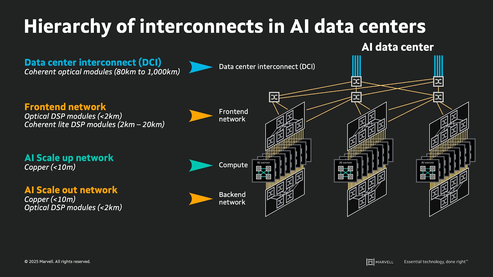
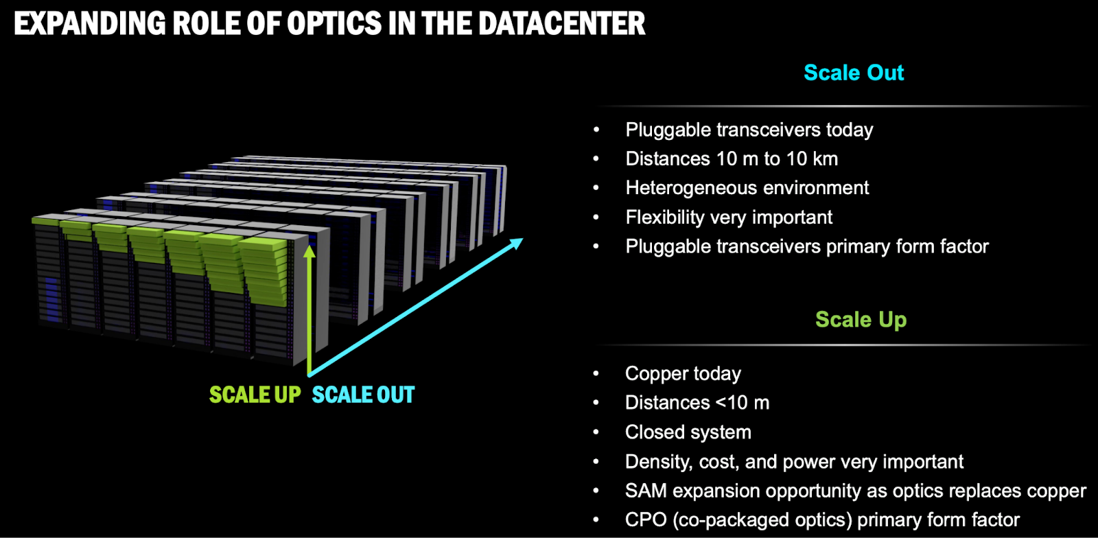
AI Networking and Scale Up vs Scale Out
Modern AI data centers adopt three types of interconnection network architectures (+ data center interconnects), each precisely tailored to different communication requirements. This multi-tiered design forms the core infrastructure for training and using large language models such as OpenAI’s GPT:
Data center interconnect (DCI or ZR): At top of the networking stack, there are data center interconnects (DCI) which span from 80km to 1,000km+ and connect multiple data centers together. Due to the long distance between each data center, coherent optical modules are used.
Front-end Network: The next layer involves a front-end network which connects the AI data center to the outer world (such as other data centers or the internet). It primarily uses the Ethernet protocol and relies on core switches, spine switches, and top-of-rack (ToR) switches to handle CPU workloads, storage access, and north-south traffic between the data center and external networks. Its transmission distance can exceed 2kms, typically via fiber connections.
AI Backend Scale-Up Network: The scale-up network is the core innovation of AI architecture, dedicated to high-speed communication between GPUs within a rack (<10m). Major vendors have developed proprietary interconnect technologies such as nVidia’s NVLink, AMD’s Infinity Fabric/UALink, Google’s ICI, and Amazon’s NeuronLink. These technologies use copper cables and PCIe interfaces to deliver nanosecond-level latency and hundreds of GB/s bandwidth. Local switches within each node coordinate the GPU fabric, enabling tight multi-GPU collaboration. This is referred to as vertical scale-up within the rack. The larger each server gets, the more powerful and performant it also gets, thus each server is scaled-up as much as possible via copper. Copper is generally the preferred choice over optics wherever possible given much higher reliability and cost efficiency, and in this case the short physical distance of these intra-rack scale-up solutions enables the use of copper. While generally passive copper fails to deliver reliable connectivity beyond 7-10 meters, active electrical cables (AECs, discussed in detail on next page) have pioneered the use of copper by up to 20 meters.
AI Backend Scale-Out Network: When the scale of AI training exceeds a single rack, the Scale-Out network becomes essential. This layer uses InfiniBand (currently mainstream) or the emerging Ultra Ethernet Consortium (UEC) standard to connect multiple racks (10-100 meters) via optical fiber or D2D copper cables (up to 20m with AECs). It integrates thousands or even tens of thousands of GPUs into a unified training cluster. Although the latency increases to the microsecond level, it remains sufficient for large-scale distributed training.If the distance is short enough (like for adjacent racks), copper can be used (up to 20 meters with AECs). The role of CPOs will grow in scale-out applications.
AI Networking within Nvidia data center:
Here is how the 3 connectivity architectures look like in a typical AI cluster. In Nvidia’s leading-edge Blackwell (NVL72 GB200), the 3 clusters include:
Within-rack scale-up network: uses Nvidia’s proprietary NVLink protocol with the 72 GPUs connected to each-other via NVSwitches using copper, there is see some role of CPO here over time as copper becomes too slow.
Inter-rack back-end or scale-out network: connects GPUs sitting across multiple racks with InfiniBand or Ethernet, this is where pluggable transceivers are used and where Nvidia recently announced availability of CPO in H2 2026 (InfiniBand) and H2 2027 (Ethernet).
Front-end network: traditional Ethernet network connecting AI cluster to the internet, also uses pluggable transceivers.
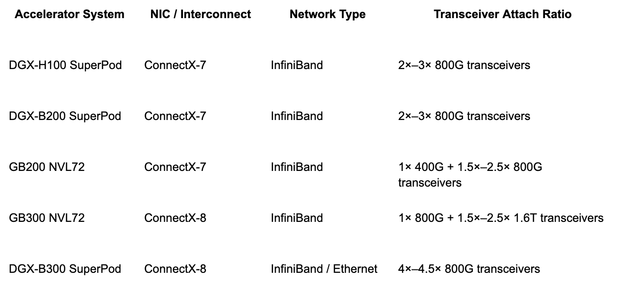
As AI chips become more powerful, transceiver attach rate goes up and how to think about the demand for transceivers:
Very importantly for optical transceiver demand, the number of transceivers needed per GPU/ASIC appears to be trending up along with the latest chip generation and networking architectures, mainly driven by upgrade to higher bandwidth in the system.
For the H100 or B200 GPU, each chip needs around 2-3x of 800G optical transceivers, however, the latest B300 GPU could need around 4-4.5x 800G optical transceivers. This increase is mainly driven by higher bandwidth in scale-out networking with the upgrade from ConnectX-7 (400G) to ConnectX-8 (800G). Even more interestingly, certain networking architecture (like DSF, disaggregated scheduled fabric) for custom ASICs suggests an attach ratio of 8x 800G transceivers per chip in training clusters.
800G optical transceiver shipment to double, substrate supply in focus:
Entering a supercycle: The ramp-up of the 800G optical transceiver modules will begin in 2025-26, with the demand expected to reach 40m units in 2026. Adoption of 1.6T modules is expected to begin in end-2025, with demand expected to exceed 20m units in 2026. The above two components are expected to deliver multiple-fold growth compared to 2025, which confirms that AI will continue to be the main driver of market growth between 2026 and 2030. Currently, CW lasers and EMLs are falling short of demand. Both domestic and international manufacturers are aggressively expanding capacity, which will help boost the sales momentum of epitaxy foundries in Taiwan. Rapid TAM growth of optical transceivers driven by AI going from $5bn in 2021 (mostly non AI) to $15bn in 2025, $20bn in 2030, $25bn in 2027, $30bn in 2028, $35bn in 2029 and $40bn in 2030.
Watch out for critical material access: In mid-2025, US-based AXT (the largest InP substrate supplier) was hit by Chinese export restrictions, making security of supply the biggest concern. Accordingly, the supply of InP substrates in 2026 is considered the major uncertainty. If China imposes another round of export controls on gallium (Ga) and germanium (Ge), certain products could effectively become impossible to manufacture. Although epitaxy foundries are aggressively certifying Japanese and European InP substrate suppliers, any tightening in supply is still likely to trigger material hoarding with negative impact on procurement. This situation requires close monitoring for its potential impact.
Market Dynamics: A Networking and Optical Supercycle
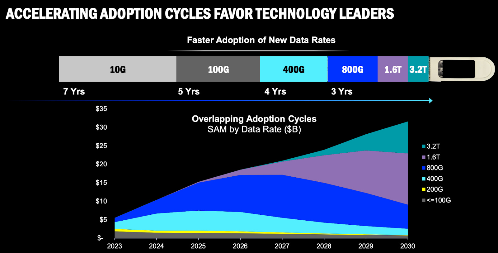
We are witnessing a supercycle because multiple technology upgrades are overlapping: Historically, the industry upgraded speeds every 3-5 years (from 100G to 400G). Now, the demand for AI is forcing 800G, 1.6T (Terabits), and 3.2T cycles to happen almost simultaneously.
The Multiplier Effect (Attach Rate): This is the most important financial metric.
In the past, one server needed one optical connection (1:1).
In modern AI clusters (like Nvidia’s H100 SuperPod), one GPU requires 3 to 5 high-speed optical transceivers. The demand for optics is growing”super-linearly relative to the demand for chips
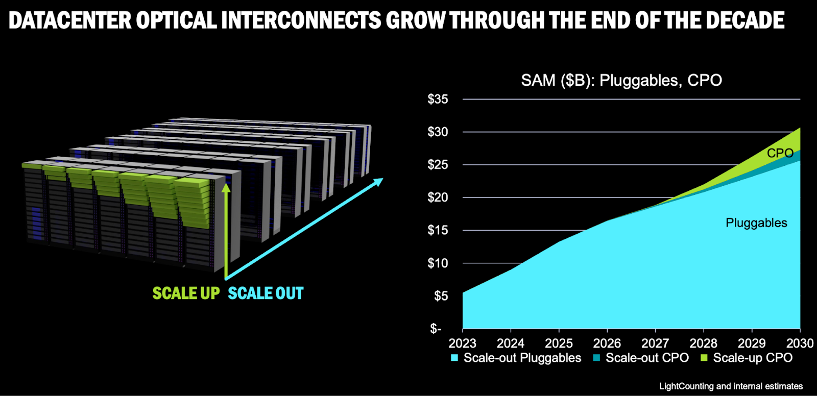
The optical connectivity market for AI could reach $30bn in 2030 and $20bn by 2028 from just $8.5bn in 2025. Pluggable optics remain the majority, but LPOs and CPOs are expected to ramp from 2026–2027.
Copper Connectivity in Data Centers
Copper is generally the preferred connectivity option in data centers whenever performance requirements allow a choice between copper and optical fiber. Compared to optics, copper solutions offer lower cost, lower latency, higher power efficiency, higher reliability, and easier deployment, at the expense of larger physical size and stricter distance limitations.
As a result, copper is predominantly used for intra-rack scale-up connectivity (e.g., server-to-ToR switch) and adjacent-rack links. While traditional copper solutions struggle to scale beyond 800G over practical distances, Active Electrical Cables (AECs) are extending copper’s viability toward 1.6T+ speeds, albeit over short reaches. AECs are widely viewed as the final practical extension of copper before a transition to optical interconnects becomes unavoidable as bandwidth and distance requirements continue to increase in large AI clusters.
Specs of Copper Connectivity in the Data Center: AECs lead high-speed copper connectivity for 800G+ applications up to 7 meters.
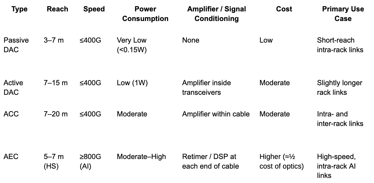
DAC - Direct Attach Cable:
Direct Attach Cables (DACs) are the simplest form of copper connectivity, with fixed transceivers at both ends. Most DACs are passive, containing no active electronics, though active DACs incorporate basic signal conditioning within the transceivers.
Passive DACs rely entirely on host-side signal processing, resulting in very low power consumption and minimal cost, but limiting reach to approximately 3-7 meters due to signal degradation. Active DACs extend reach to roughly 10-15 meters, but remain constrained in bandwidth scalability and physical bulk. As a result, both passive and active DACs are poorly suited for dense, high-speed AI racks with dozens to hundreds of GPUs.
ACC - Active Copper Cable:
Active Copper Cables (ACCs) integrate active electronics, such as signal drivers, directly into the cable to compensate for signal loss over longer copper runs. ACCs enable extended reach (up to 20 meters) while remaining copper-based and are typically used for intra-rack or adjacent-rack connectivity.
However, ACCs do not fully eliminate signal degradation as distance increases, and noise accumulation ultimately limits achievable bandwidth and signal integrity, particularly at higher data rates.
AEC - Active Electrical Cable:
Active Electrical Cables (AECs) represent the most advanced form of copper connectivity, incorporating retimers (CDRs) or DSPs at both ends of the cable. These devices actively re-clock, re-shape, and clean the signal, removing accumulated noise and jitter and enabling reliable operation at 800G and beyond.
AECs were pioneered commercially by Credo with the first 800G AEC deployments at Microsoft in 2021. Current-generation AECs support 800G (8 × 112G lanes) over reaches of up to 7 meters and are increasingly adopted for intra-rack scale-up AI architectures. Ongoing R&D is targeting 20-meter AECs, which would enable selective rack-to-rack copper connectivity.
AECs also support disaggregated and distributed chassis architectures, allowing greater flexibility in server and switch configurations and reducing operational complexity in hyperscale data center builds.
Credo (CRDO) is the clear market leader, with major customers including Microsoft, Amazon, and xAI. New entrants such as Marvell (MRVL) are expected to gain share over time. Notably, Credo sells integrated cable-plus-electronics solutions, while competitors typically supply DSPs to cable and connector vendors such as Amphenol and Molex.
Optical Connectivity in Data Centers
While copper dominates short-distance chip-to-chip or chip-to-switch connectivity (e.g., NVIDIA NVLink), optical fiber is essential for front-end, inter-node, inter-rack (scale-out), and inter-data center (DCI) connectivity.
Optical connectivity trades higher cost and complexity for greater reach, bandwidth, and scalability, making it critical for AI and cloud-scale workloads. Types of optical solutions include:
Pluggable transceivers (traditional modules with DSPs)
Linear Receive Optics (LROs)
Linear Pluggable Optics (LPOs)
Co-Packaged Optics (CPOs)
These devices integrate transmitters, receivers, and silicon photonics technology, enabling high performance, energy efficiency, and dense scaling. Unlike RF or consumer transceivers, optical modules are optimized for speed, density, and power efficiency in hyperscale data centers.
Specs of Optical Connectivity in the Data Center: CPOs offer materially better power efficiency versus traditional DSP-based architectures such as pluggable optics and LPOs.
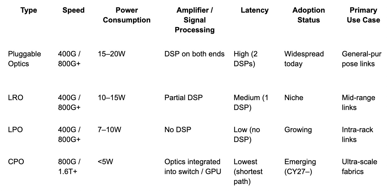
Pluggable Optics - DSP on both ends:
Pluggables are industry-standard optical transceivers. Each module integrates a laser, transimpedance amplifier (TIA), driver, and DSP to correct signal degradation over fiber.
Advantages:
Widespread adoption and easy deployment
Long reach and high reliability
Disadvantages:
High power consumption (15–20W)
Higher latency due to DSP processing
Pluggables remain the majority of optical connectivity solutions through 2030.
LRO (Linear Receive Optics) - DSP on one end:
LROs remove the DSP on the receive side, relying on the transmit-side DSP for signal integrity.
Advantages:
Reduced power and latency compared to pluggables
Disadvantages:
Limited reach, low interoperability, and niche adoption
LPO (Linear Pluggable Optics) - no DSP:
LPOs eliminate DSPs entirely, using linear amplifiers and host ASIC equalization.
Advantages:
50% power reduction vs. pluggables
Low latency, cost-efficient
Disadvantages:
Shorter reach, low standardization, niche adoption
CPO (Co-Packaged Optics) - integrated optics (no DSP):
CPOs integrate optics directly into the ASIC or switch (via 2.5D / 3D packaging), eliminating discrete transceiver modules.
Advantages:
Very high bandwidth density
Up to 3.5x lower power than traditional pluggables
Minimal latency due to short signal paths
Disadvantages:
High cost, complex IP, emerging technology
Power efficiency:
Pluggable: 30W per module (20W DSP, 10W laser)
CPO: 9W total (7W optical engine, 2W CW laser)
CPOs are expected to ramp in hyperscale AI data centers as optical power could reach 10% of total compute power.
For CPOs specifically, Nvidia has its own CPO-integrated switch offerings for InfiniBand (Quantum-X, H2 2026) and Ethernet (Spectrum-X, H2 2027) which could help drive initial adoption, along with Broadcom’s CPO offerings in 2027.
ZR/ZR+:
ZR/ZR+ is an application rather than a type of optics, typically using coherent pluggable modules with DSPs for long distances.
Market dynamics (Marvell forecast):
DCI interconnect TAM: $1.0B (2023): $3.0B (2028), CAGR +25%
Existing DCI (120 km): $2B opportunity
New ultra-large DCI (1,000 km+): $1B opportunity
Products: Marvell Orion 800G coherent DSP and CORORZ 800 ZR/ZR+ pluggables, with 1.6T variants expected
ZR/ZR+ adoption will accelerate multi-site AI workloads and large-scale optical data center interconnects.
What is Optical Connectivity?
Leveraging the speed of light to carry information: At a simplistic level, optical communication is the conversion of an electrical signal carrying digital information generated by a device into an optical signal, which is then routed to a specific destination, where it is then converted back to an electrical signal, which enables the receiving device to consume the digital information.
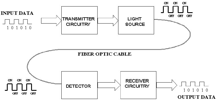
Optical transmission in modern data centers depends on efficient conversion between electrical and optical domains. This includes the light source (lasers), receivers, transceivers, and transport components that enable high‑speed, long‑distance data movement with low error rates and high reliability.
Transmission: Generating and Receiving Signals
Laser: Converting an Electrical Signal into Optical
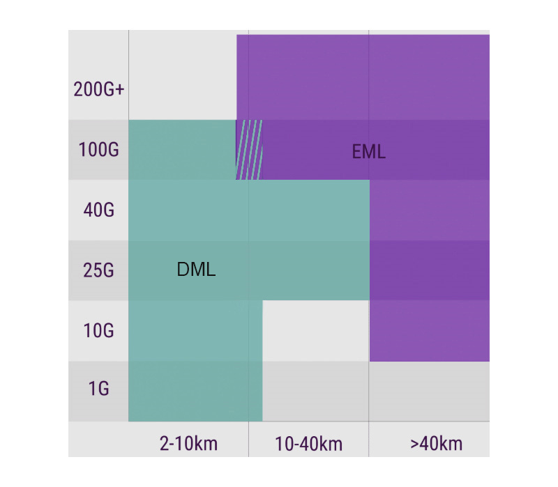
Not all lasers are created equal. The light source of an optical network is a core and critical component for fiber optic transmission and must meet several criteria, including wavelength, modulation and power requirements, in order to transmit data efficiently for any particular use case. While lasers have been proven to be the light source of choice, given high bandwidth and narrow spectral output, not all lasers are the same and thus there are multiple types leveraged in the market, such as:
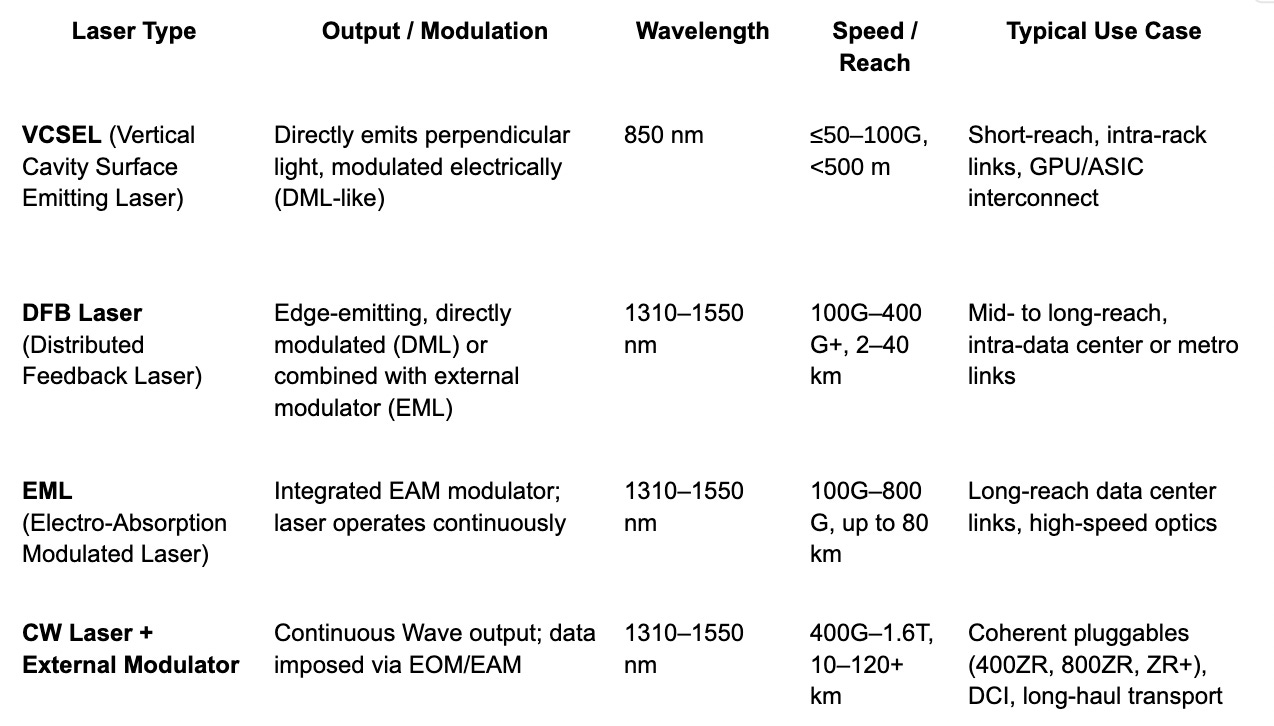
Modulation is key when it comes to DML and EML
DML: Simple direct modulation; lower cost and power; short reach.
EML: Laser with integrated modulator; supports higher speeds and longer reach.
CW + Modulator: Continuous output laser with external modulator; required for coherent pluggables and long-reach DCI.
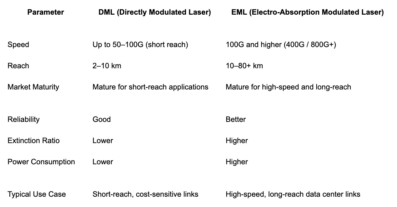
The use of a DML vs. EML is largely based on cost and power consumption vs. data rate and distance. However, the choice is typically a simple one given the technical limitations restricting the use of DMLs for certain distances, and the higher cost making the use of EMLs economically infeasible for lower data rates and shorter distances, however, there are certain areas in which use cases overlap.
Receiver: Converting an Optical Signal into Electrical
The optical receiver is a core component of fiber-optic communication systems.
Receivers are critical for signal fidelity. They typically include:
Photodetector: Converts optical power into an electrical current.
Transimpedance Amplifier (TIA): Amplifies the signal to a usable level.
Signal Processing / DSP: Performs noise compensation, chromatic dispersion correction, and equalization.
Materials:
Silicon photonics (Si) for short to mid-reach (<10 km).
Indium Gallium Arsenide (InGaAs) for high sensitivity, long-reach coherent links (1310–1550 nm).
Transceivers: Combining Laser and Receiver
An optical transceiver integrates both transmission and reception functions within a single module. The core optoelectronic components traditionally consist of a Transmit Optical Sub-Assembly (TOSA) and a Receiver Optical Sub-Assembly (ROSA), housed alongside control electronics and a printed circuit board.
Transmit Optical Sub-Assembly (TOSA): Responsible for converting electrical signals into optical signals. It typically includes a laser diode, optical interface, monitor photodiode, housing, and electrical interface.
Receiver Optical Sub-Assembly (ROSA): Responsible for converting incoming optical signals into electrical signals. It typically includes a photodiode, optical interface, housing, and electrical interface.
In advanced architectures such as silicon photonics and co-packaged optics, these functions are increasingly integrated, reducing reliance on discrete sub-assemblies.
Transceiver Form Factors and Use Cases
Not all transceivers are identical, as performance, power, and cost requirements vary by application. Common form factors include:
SFP / SFP28 / SFP56: Compact, hot-pluggable modules used for 10G, 25G, and 50G links. Hot pluggable refers to a device that can be added or removed from a network without shutting down the network.
QSFP / QSFP28 / QSFP56: Four-lane pluggable modules supporting 100G and 200G.
QSFP-DD and OSFP: High-density form factors enabling 400G and 800G deployments in hyperscale data centers.
CFP variants: Larger form factors primarily used in long-haul and telecom applications, with limited relevance in modern data center environments.
Coherent Technology and Coherent Transceivers
What is coherent technology and how does it work?
Coherent optical technology increases the amount of data transmitted over a single wavelength by leveraging multiple properties of light, including amplitude, phase, and polarization. This approach enables substantially higher spectral efficiency compared to traditional direct-detect systems and supports applications ranging from ultra-long-haul transmission to metro networks and data center interconnects.
Traditional non-coherent transceivers encode data using changes in optical intensity, representing binary values through the presence or absence of light. Coherent technology, by contrast, encodes information across multiple signal dimensions and relies on coherent detection to recover the transmitted data, enabling significantly higher data rates over existing fiber infrastructure.
Components of coherent transceivers
Coherent transceivers rely on several specialized components, including high-performance digital signal processors (DSPs), photonic integrated circuits (PICs), and control electronics. The DSP performs complex modulation, demodulation, and signal correction functions, while the PIC integrates optical modulation and coherent reception, measuring both signal intensity and phase.
As data rates increase, DSP power consumption and thermal management have become the primary constraints in coherent transceiver design. Silicon photonics has emerged as the dominant platform for PIC integration.
Baud rate and QAM modulation
Increasing baud rate alone is insufficient to meet rising bandwidth demand. Modern coherent systems increase bit rates by combining higher symbol rates with higher-order modulation schemes such as quadrature amplitude modulation (QAM). Dual-polarization QAM enables multiple bits per symbol by encoding data across both polarization states.
Higher-order modulation schemes such as 64 QAM and 128 QAM enable data rates of 400G, 800G, and beyond, but require higher signal-to-noise ratios and increasingly sophisticated DSPs, increasing system cost and power consumption.
ACO vs. DCO Architectures
Coherent transceivers are commonly categorized based on DSP placement. In analog coherent optics (ACO), the DSP resides in the host system, while in digital coherent optics (DCO), the DSP is integrated within the transceiver module. In modern deployments, DCO architectures dominate due to their modularity and compatibility with router-based and switch-based coherent networking.
Coherent vs. Non-Coherent Technologies
Non-coherent (direct-detect) technologies offer lower cost and power consumption but are constrained in achievable reach and data rate. Coherent technologies enable significantly higher spectral efficiency and longer reach but at higher cost and power. As data rates increase and link distances extend, coherent solutions are increasingly favored despite their higher complexity.
Pluggable coherent transceivers and ZR standards
Pluggable transceivers integrate all optical and electronic components into hot-pluggable modules, enabling flexible deployment and simplified maintenance. Standards such as 400G ZR define interoperable coherent pluggables capable of supporting data center interconnect links up to 100 km using compact form factors such as QSFP-DD and OSFP.
The adoption of pluggable coherent optics is driving a shift away from proprietary DWDM systems toward more open, router-based optical architectures, significantly reducing cost per bit.
Transport Market: Managing Signals
Optical transport components:
Reconfigurable optical add/drop multiplexers (ROADMs) enable dynamic wavelength routing in optical networks, improving flexibility and reducing over-provisioning. Optical amplifiers, including erbium-doped fiber amplifiers (EDFAs) and Raman amplifiers, extend transmission distances without optical-to-electrical conversion. EDFAs remain the dominant amplification technology due to cost and maturity, often supplemented by Raman amplification in long-haul systems.
Multiplexers and demultiplexers combine and separate wavelengths, enabling dense wavelength-division multiplexing over a single fiber.
Transport Market: Managing Signals
ROADM: Routing Optical Network Traffic
What is a ROADM?
A reconfigurable optical add/drop multiplexer (ROADM) consists of a wavelength selective switch (WSS), which is an active component that enables the user to dynamically route any wavelength to and from any port.
Other components include an optical channel monitoring (OCM), which monitors the optical power of each wavelength, and a variable optic attenuator (VOAs), which configures the attenuation of optical power in each wavelength.
What does a ROADM (Reconfigurable Optical Add/Drop Multiplexers) do?
Optical networks must leverage architectures that route data traffic from long-haul networks to metro networks without sacrificing speed or capacity. However, historically optical networks were fixed and difficult to change and had to design their networks while trying to anticipate where traffic would be flowing for the upcoming year as well as ten years beyond that driving inefficiencies in traffic routing and overbuilding capacity. However, by deploying a ROADM, a network can remotely switch traffic by adding, blocking, passing or redirecting wavelengths of light in real-time. Importantly, this approach is more flexible and less expensive than older approaches requiring converting optical to electrical signals and back again.
Amplifiers: Enabling Longer Distances for Optical Signals
What is an optical amplifier?
The transmission loss of the light passing through an optical fiber is very small over short distances; however, when the distance expands as far as 10 km or greater, the transmission loss can be material. Thus, an optical amplifier boosts or “amplifies” the optical signals passing on a fiber through the way of directly stimulating the photons of the signal with extra energy, without converting it back to electrical signal, which enables it to travel longer distances.
Different types of optical amplifiers: OFA & SOA
There are two types of optical amplifiers: Optical Fiber Amplifier (OFA) and Semiconductor Optical Amplifier (SOA). Within OFA, there are an additional two types: Erbium-Doped Fiber Amplifier (EDFA) and Fiber Raman Amplifier (FRA).
EDFA (Erbium-Doped Fiber Amplifier): Most common; low cost, high gain, widely deployed.
Raman Amplifier (FRA): Wideband, distributed gain; used in long-haul systems.
SOA (Semiconductor Optical Amplifier): Compact, electrically pumped; niche applications.
EDFA remains dominant technology on cost and meeting current requirements
While the overall performance of a FRA is better than an EDFA given: 1) it has a wide band; and 2) it enables distributed amplification within the transmission fiber (like increase the length of spans between the amplifiers and regeneration sites), an EDFA meets most of the current requirements in the market while also boasting a lower cost, high pump power utilization, good gain stability and high gain with little cross-talk.
Mux/DeMux: Combining and Separating Wavelengths
What is a Mux/DeMux Filter?
Multiplexer (Mux): Combines multiple wavelengths onto a single fiber.
Demultiplexer (DeMux): Separates composite fiber signal into individual wavelengths.
Key for dense WDM networks in DCs and DCI.
The Rise of Silicon Photonics
The exponential growth of Large Language Models (LLMs) has shifted the primary bottleneck in data centers from computation to data movement. As electrical interconnects (copper) hit physical limitations regarding bandwidth density and power consumption, the industry is transitioning to Silicon Photonics (SiPh). This technology integrates optical and electronic components onto a single silicon chip, enabling the manipulation of light at micro and nanoscale dimensions.
1. The Core Technology: Silicon Photonics (SiPh)
Silicon photonics is the convergence of high-speed optics with established CMOS (Complementary Metal-Oxide-Semiconductor) manufacturing. Unlike traditional discrete optical components, SiPh fabricates photonic functions directly onto silicon wafers.
Mechanism: It separates light generation from signal modulation. A Continuous Wave (CW) laser provides a constant light source, while the silicon chip uses modulators to encode data onto that light,.
Key Benefits:
Energy Efficiency: Reduces power consumption by up to 80% compared to traditional interconnects (3.5pJ/bit vs. 10-20pJ/bit).
Throughput: Supports data rates up to 1.6Tbps, roughly 16x higher than standard copper interconnects.
Scale: Leverages mature 300mm CMOS manufacturing ecosystems for high yields and lower costs.
2. Critical Materials & Substrates
The performance of an optical system depends heavily on the underlying substrate material.
Photonics-SOI (Silicon-on-Insulator): The current industry standard. These wafers feature a top crystalline silicon layer (patterned into waveguides to carry light) and a buried oxide layer (BOX) for optical confinement. It dominates roughly 90% of the SiPh wafer market.
Indium Phosphide (InP): The “active” material. Because silicon cannot emit light, InP is essential for the laser diodes (light sources) and amplifiers. It is currently the only material capable of integrating active components like lasers directly on-chip, though it remains brittle and complex to manufacture.
LNOI (Lithium Niobate on Insulator): The emerging contender for ultra-high bandwidth. LNOI offers superior electro-optic modulation efficiency (low optical loss), making it critical for future 3.2Tbps pluggable modules expected around 2027–2028,.
SiGe (Silicon Germanium): Primarily used for photodetectors (converting light back into electricity) within the Photonic Integrated Circuit (PIC).
3. The Fundamental Unit: The Photonic Integrated Circuit (PIC)
The PIC is the optical equivalent of a computer processor. Instead of transistors, it consolidates multiple photonic functions into a single die.
Waveguides: Passive channels that guide light across the chip.
Modulators: Active components that imprint electrical data onto the light stream.
Photodetectors: Sensors that receive optical signals and convert them back into electrical data.
4. Architectural Evolution: From Pluggables to Optical I/O
The physical location of the optics relative to the processing chip (ASIC or GPU) defines the architecture. The industry is moving the optics closer to the processor to reduce the “electrical distance” signals must travel.
A. Pluggable Optical Transceivers (Current Standard)
Function: Modules plugged into the front panel of a switch. They convert electrical signals from the switch into optical signals for transport.
Status: The mainstream technology for speeds from 400G to 1.6Tbps.
limitation: As speeds hit 6.4Tbps, the electrical resistance between the switch chip and the front panel creates untenable power consumption and thermal management issues.
B. Co-Packaged Optics (CPO) (The Near Future)
Function: Moves the optical engine away from the front panel and mounts it directly onto the same substrate/package as the switch ASIC.
Benefit: Drastically shortens the electrical link, reducing power consumption and latency while increasing bandwidth density.
Timeline: Expected to ramp meaningfully around 2027–2028 as the industry moves to 51.2T and 102.4T switches. It is seen as the solution for Scale-Out architectures (switch-to-switch).
C. Optical I/O (The Holy Grail)
Function: Replaces the electrical pins on a processor with optical connections. This brings fiber directly to the xPU (GPU/CPU/ASIC).
Use Case: Critical for Scale-Up architectures (chip-to-chip or memory-to-chip communication within a server rack). It solves the bottleneck of interconnecting thousands of GPUs for AI training.
Tech Enabler: Requires advanced 3D packaging, such as TSMC’s COUPE (Compact Universal Photonic Engine), which stacks the electrical die (EIC) on top of the photonic die (PIC) to minimize impedance.
5. Key Manufacturing Processes
Epitaxy (Epi-wafer): The decomposition of compound materials (like InP or GaAs) over a substrate to create the active laser layers. This is the highest barrier-to-entry step in the supply chain.
Hybrid Bonding: The process of vertically stacking and connecting the electronic control chip (EIC) and the photonic chip (PIC) with extreme precision. This is essential for next-gen CPO and Optical I/O performance.
Coupling: The physical connection of the fiber optic cable to the chip using Fiber Array Units (FAUs). This remains a major yield challenge due to the high precision required.
Optical Circuit Switching: MEMS vs. Liquid Crystal
As AI data centers scale to support 100,000+ GPU clusters, Optical Circuit Switching (OCS) has emerged as a critical technology for reducing power consumption, latency, and cost. Unlike traditional electrical packet switches, OCS creates direct optical paths between ports without optical-electrical-optical (OEO) conversion. Google has catalyzed market interest by deploying tens of thousands of OCS ports internally, demonstrating 40% power savings and 30% cost savings compared to traditional electrical switching. The OCS market is projected to exceed $2.5 billion by 2029, with multiple technology approaches competing for dominance.
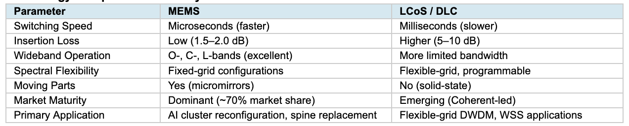
The Two Primary Technologies: MEMS and Liquid Crystal (LCoS)
Two dominant switching technologies are vying for market share: MEMS-based switches and Liquid Crystal on Silicon (LCoS). Each technology has distinct advantages suited to different applications, and hyperscalers are evaluating both based on their specific infrastructure requirements.
MEMS (Micro-Electro-Mechanical Systems):
MEMS-based OCS uses arrays of microscopic mirrors fabricated on silicon substrates. In 3D MEMS configurations, mirrors tilt continuously along two axes, directing light beams from input fibers to any output fiber across the switching fabric. This approach currently dominates the market, accounting for over 70% of OCS deployments.
Switching Speed: Microsecond-range reconfiguration (faster than LCoS), making it suitable for latency-sensitive applications requiring rapid network reconfiguration.
Insertion Loss: Very low (typically 1.5–2.0 dB for 300x300 port switches), as MEMS relies on direct reflection with minimal optical path complexity.
Bandwidth Transparency: Operates seamlessly across O-, C-, and L-bands, making it future-proof for 400G, 800G, and 1.6T links without requiring upgrades.
Reliability: Single-crystal silicon designs eliminate “hinge fatigue,” enabling hundreds of millions of operational cycles. Lumentum claims over 1 trillion field mirror operating hours across their deployed base.
Scalability: Proven at scale up to 300x300 ports (Lumentum R300) with 1,100+ port switches demonstrated in research. Higher port counts require increasingly complex free-space optical designs.
Key Players: Lumentum (R300, R64), Calient, DiCon, and Google (internal). Lumentum has guided to approximately $100 million per quarter in OCS revenue by end of 2026.
Liquid Crystal on Silicon (LCoS) / Digital Liquid Crystal (DLC):
LCoS-based switches use reflective spatial light modulators where liquid crystal cells modulate light phase based on electrical signals, enabling beam steering without mechanical movement. This technology leverages mature display manufacturing processes.
Switching Speed: Millisecond-range reconfiguration due to liquid crystal viscoelastic properties (refresh rates typically limited to a few hundred hertz). Slower than MEMS but sufficient for many static or semi-static network configurations.
Insertion Loss: Higher than MEMS (typically 5–10 dB) due to diffraction effects and polarization sensitivity, requiring additional polarization diversity optics.
Spectral Flexibility: Pixel-level control enables highly flexible wavelength selection and software-programmable channel configurations, critical for flexible-grid architectures in DWDM networks.
Reliability: No moving mechanical parts, offering excellent long-term reliability. However, performance can be temperature-sensitive.
Scalability: Two-dimensional beam steering supports higher port counts more easily than MEMS. Liquid crystals scale naturally in pixel number, but small steering angles limit practical port counts without complex optical designs.
Key Players: Coherent is the primary developer of Digital Liquid Crystal (DLC) OCS solutions, currently introducing products into the hyperscaler supply chain.
Technology Comparison Summary:
Investment Implications:
MEMS currently leads the OCS market for AI data center applications due to superior switching speed, lower insertion loss, and wideband operation. Lumentum is the clear leader, with public guidance suggesting it could capture roughly half the OCS market in 2026. The July 2025 formation of the OCP OCS sub-project (founding members include Lumentum, Google, Microsoft, Nvidia, and Coherent) signals industry-wide commitment to standardization and accelerated adoption.
Coherent’s DLC approach offers an alternative path, particularly for applications requiring flexible wavelength management. As OCS adoption expands beyond Google to Microsoft, Amazon, and other hyperscalers, both technologies are likely to find their niches: MEMS for high-speed AI cluster reconfiguration and spine-layer replacement, and LCoS/DLC for flexible-grid DWDM and wavelength-selective switching applications. The combined OCS market represents a significant new opportunity within the broader optical networking supercycle.
CPO: The Future of Optical Connectivity
Eliminating the Electrical Desert: In traditional data center architectures, data travels as electricity from the switch chip (ASIC) across a printed circuit board (PCB) to the front panel, where it enters a pluggable optical transceiver to be converted into light. As speeds increase to 1.6T and 3.2T, this short journey (approximately 6–10 inches) becomes a bottleneck. The copper traces act as heaters, causing signal loss and consuming excessive power just to push the electrons to the edge of the box.
Co-Packaged Optics (CPO) solves this by moving the optical engine off the front panel and integrating it directly onto the same package substrate as the switch ASIC or xPU (GPU/CPU). This reduces the electrical path to mere millimeters, effectively bypassing the PCB.
Key Technical Components CPO is not a single widget but a convergence of technologies:
Silicon Photonics (SiPh): The enabling platform. It uses standard CMOS manufacturing to print optical circuits (waveguides, modulators) directly onto silicon wafers. SiPh separates “light generation” from “signal modulation”.
The Optical Engine (OE): This is the heart of CPO. It consists of a Photonic Integrated Circuit (PIC) stacked with an Electronic Integrated Circuit (EIC), often using advanced Hybrid Bonding (like TSMC’s COUPE platform) to connect them vertically.
External Laser Source (ELS): Silicon cannot emit light, and lasers degrade quickly in high-heat environments. Therefore, CPO uses “Remote” or “External” light sources. The lasers (Continuous Wave or CW Lasers) remain as pluggable modules on the front panel, sending light through fiber cables into the hot ASIC package where the modulation occurs. This ensures the lasers can be easily replaced if they fail.
Use Cases: Scale-Out vs. Scale-Up CPO serves two distinct architectural needs in AI clusters:
Scale-Out (The Network): Connecting racks of servers via switches (Ethernet/InfiniBand). This is the first wave of CPO adoption, led by Broadcom (Tomahawk 5 “Bailly”) and Nvidia (Quantum-X800). It targets the 51.2T and 102.4T switch generations.
Scale-Up (The Compute): Connecting GPUs to memory or other GPUs (e.g., NVLink). This is considered the “holy grail” because the volume of connections is 10x higher than in switches. However, due to extreme thermal density near the GPU, this adoption is expected to trail switch-based CPO, likely arriving between 2028–2030.
Market Potential & Timeline
The Inflection Point: 2027–2028 While early deployments of CPO switches (like Broadcom’s Bailly) are beginning, widespread commercial adoption is tied to the 3.2T transceiver generation:
Near Term (2025–2026): Pluggable modules (1.6T) will remain dominant. CPO will see trialling to establish reliability and interoperability.
Inflection (2027+): As the industry moves to 3.2T speeds, pluggables hit physical thermal limits. This is when CPO is expected to ramp meaningfully.
Market Size Estimates:
Base Case: The CPO market is forecast to reach approximately $5-$7 billion by 2030.
Upside Case: If AI compute scaling accelerates demand for Scale-Up optical interconnects (optical I/O), the total addressable market (TAM) could reach upwards of $14 billion by 2030, representing 25% of the total optical transceiver market.
Silicon Photonics: As the underlying technology for both CPO and next-gen pluggables, the SiPh wafer/chip market is expected to grow at a 35% CAGR, reaching $4–$6 billion by 2028–2030.
Supply Chain Disruption: The Value Shift CPO shifts value away from traditional module assemblers toward semiconductor foundries and advanced packagers.
The Winners:
Foundries: TSMC is the critical enabler with its COUPE (Compact Universal Photonic Engine) platform.
Packaging: ASE and Amkor are positioned to capture value in assembling these complex optical-electrical packages.
Equipment: Besi is the leader in hybrid bonding tools required to stack the EIC on the PIC.
Lasers: Lumentum and Coherent remain vital as suppliers of the high-power CW lasers (ELS) required to power these systems.
The Risk: Traditional transceiver assemblers (who currently build the pluggables) face a terminal risk if they cannot pivot to becoming component suppliers or contract manufacturers for the ELS modules.
Disclaimer: The information provided on this Substack is for general informational and educational purposes only, and should not be construed as investment advice. Nothing produced here should be considered a recommendation to buy or sell any particular security.
 | A guest post by
|